introduction
In the age of multimedia, traditional Class A, Class B, Class AB linear analog audio amplifiers can no longer meet new developments such as green energy saving, high efficiency, and small size of electronic audiovisual LCD / PDP / OLED / LCOS / PDA due to their low efficiency and large energy consumption. Trends, and Class-D power amplifiers for nonlinear audio amplifiers will be incorporated into more and more new product designs due to their advantages of energy saving, high efficiency, high output power, low temperature rise effect, and small footprint. The class D amplifier architecture is divided into half-bridge asymmetric and full-bridge symmetrical types, while the full-bridge type has up to 4 times the output power of the half-bridge type, which is more efficient; from the signal adaptation, it is divided into analog and I2S all-digital types. Because the all-digital type is still in the development stage and the cost is high, the analog type will be in the mainstream of application in the next few years due to cost advantages. This article focuses on the analysis of the design elements of the full-bridge analog class D amplifier, and implements a TFA9810T circuit design based on NXP's new green energy efficiency analog class D amplifier. It focuses on green energy saving and high efficiency, high output power, low temperature rise effect, PCB layout, Summarize and analyze several aspects of EMI suppression.
1 Class D power amplifier principle characteristics
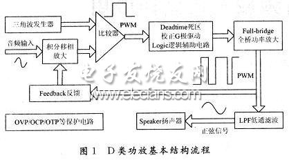
1.1 Class D amplifier system structure
Class D amplifier is composed of integral phase-shifting, PWM modulation module, G-gate drive, switching MOSFET circuit, Logic auxiliary, output filtering, negative feedback, protection circuit and so on. In the process, the analog input signal is first modulated into a PWM square wave signal. The modulated PWM signal drives the power output stage through the drive circuit, and then filters out the high-frequency carrier signal through low-pass filtering. The original signal is restored and the speaker is driven to sound, as shown in the figure 1 shown.
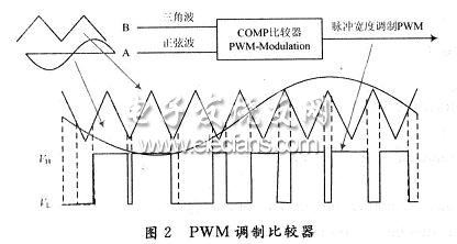
1.2 Modulation level (PWM-ModulaTIon)
The modulation stage is A / D conversion, which samples the input analog audio signal to form a high-low level digital PWM signal. In Figure 2, the non-inverting input of the comparator is connected to the audio signal source, and the reverse is connected to the triangle wave signal generated by the internal clock of the power amplifier. When the signal level of the audio input terminal is higher than the triangle wave signal, the comparator outputs a high level VH, otherwise, it outputs a low level VL, and converts the input sine wave signal into a PWM wave whose width changes with the amplitude of the sine wave. This is one of the cores of Class D power amplifiers. It must require good linearity of the triangle wave, stable oscillation frequency, high precision of the comparator, and fast speed. The generated PWM square wave has steep rising and falling edges. For in-depth modulation measures, see [2].
1. 3 full bridge output stage
The output stage is a switching amplifier with an output swing of VCC. The circuit structure is shown in Figure 3. The MOSFET is equivalent to an ideal switch. When it is turned off, the on-current is zero and there is no power consumption; when it is turned on, the voltage at both ends is still close to zero. Although there is current, the power consumption is still close to zero; the entire work During the cycle, the MOSFET basically has no power consumption, so in theory the conversion efficiency of the class D amplifier can be close to 100%, but considering the auxiliary circuit power consumption and MOSFET conduction loss, the overall conversion efficiency can generally reach about 90%. Because the conversion efficiency is very high, the heat energy consumed by the chip itself is small, and the temperature rise is also very small. It is completely possible to disregard poor heat dissipation, so it is called a green energy efficiency Class D amplifier.
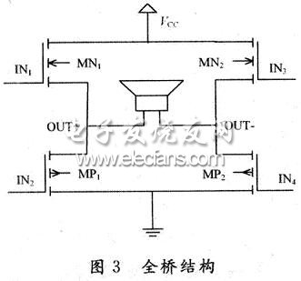
For the full bridge, to further reduce the conduction loss, it is necessary to make the on-resistance RON of the MOSFET drain source as small as possible. Select MOSFETs with low switching frequency and small gate-source capacitance to enhance the driving capability of the pre-driver.
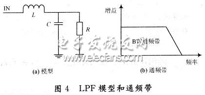
1.4 LPF low-pass filter stage
The LPF filter can eliminate electromagnetic interference and switching signals in the PWM signal, improve efficiency, reduce harmonic distortion, and directly affect the amplifier bandwidth and THD. A proper cut-off frequency and filter roll-off coefficient must be set to ensure audio quality. For audiovisual products, 20 Hz to 20 kHz is audible sound; below 20 Hz is infrasound; above 20 kHz is ultrasound. The cut-off frequency is generally set to 30 kHz in applications. The lower the frequency, the narrower the signal bandwidth, but too low will damage the signal quality, too high will cause noise to mix in. Commonly used LPF filters generally have three types: Butterworth filter, Chebyshev filter, and Kaul filter. Butterworth filters have good maximum flat amplitude characteristics in the passband BW and are easy to implement. Therefore, audio-visual products mostly use LC second-order Butterworth filters with small equivalent internal resistance and large output power.
1.5 Negative feedback
Negative feedback is an LPF circuit that feeds back the detected audio components of the output stage to the input stage. Comparing with the input signal, the output signal is compensated, corrected, and noise shaped to improve the linearity of the power amplifier and reduce the ripple in the power supply (power supply suppression) Than PSRR). Negative feedback can reduce the noise caused by pulse width modulation, output stage and power supply voltage changes in the passband, so that the low-frequency components in the output PWM can always be consistent with the input signal to get a good THD and make the sound more rich and accurate.
1.6 Power consumption efficiency analysis
The efficiency of Class D can reach more than 85% when THD <7%, which is much higher than the linear power amplifier with a maximum theoretical efficiency of 78.5%. The fundamental reason is that the output stage MOSFET is fully working in the switching state. Theoretically, the efficiency of Class D amplifier is:
Assuming that the on-resistance of the Class D power amplifier MOSFET is RON, all other passive resistances are RP, the filter resistance is RF, and the load resistance is RL, then the efficiency without considering the switching loss is:
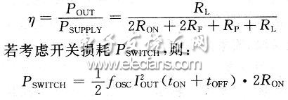
Where: fOSC is the oscillator frequency; tON and tOFF are the MOSFET on and off frequencies, respectively. The efficiency at this time is:
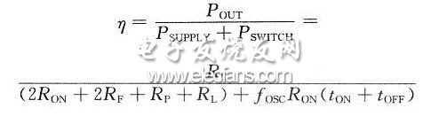
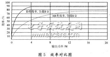
According to the above formula, the load RL in the class D amplifier is larger than the other resistors. The larger the ratio, the higher the efficiency. The power consumed by the MOSFET as a freewheeling switch is almost equal to the sum of the I2RON loss and quiescent current on the MOSFET on-resistance. The power output to the load is almost negligible. Therefore, its efficiency is much higher than the linear power amplifier, as shown in Figure 5. It is very suitable for the requirements of today's green energy saving, and it is suitable for large-scale use of digital audio-visual products such as tablets.
USB Charger Cable advantage:
For iPhone Cable Charger High Quality Usb Data Line 2.1A Fast Charging USB Cable For Apple Charging Chord For phones Charger
100% Brand new and high quality.Feel smooth, tough and durable,Original quality cable for smart phone.Set bracket, lightning charging solid data line, copper wire specifications, charging 2 core *25*0.1, data 2 core *12*0.1 74 copper wire.

Usb Charger Cable,Usb Charging Cable,Usb Cable Charging Cable,Micro Usb Charger Cable
Dongguan City Leya Electronic Technology Co. Ltd , https://www.dgleya.com