The FloorPlanning tool is an integral part of PlanAhead, which allows you to analyze FPGA designs by first finding timing or congestion issues in your design and then using PloorPlanning constraints to guide the implementation tool to produce better results. For example, using LOC constraints can lock a logical object in a Pblock (Phisical Block Region) to a location or to a region.
In order to use FloorPlanning effectively, you must have a deep understanding of Xilinx's device structure. If you are not familiar with the device structure, the layout constraints generated by the FloorPlanning tool will not improve the design performance, and in many cases will degrade the system performance. With FloorPlanning for layout planning, there is no ready-made, “correct†planning solution, but multiple attempts by designers to find a reasonable planning solution.
1. Specify key logic into the Pblock.
Here we continue to use the example used in Section 10.5. As can be seen from the timing analysis in Figure 10-68, this design has multiple timing violations, mainly the usbEngine0 and usbEngine1 modules. In fact, the timing can be converged in a variety of ways. We will only introduce a method for timing closure using FloorPlanning. In the [Netlist] window, select the usbEngine0 module, select [Draw Pblock] in its right-click menu, use the left mouse button to draw a rectangle in the [Device] window, and drag the mouse to adjust the size of the rectangle so that it can accommodate all usbEngine0. Required resources. As shown in Figure 10-75. Create a Pblock for usbEngine1 in the same way.
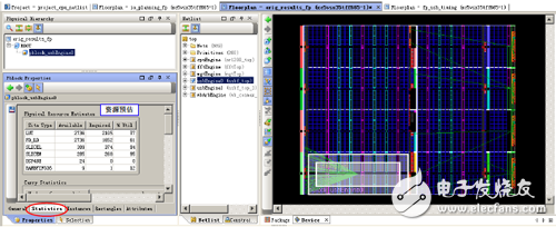
Figure 10-75 Creating a Pblock
2. Manually add LOC location constraints.
Run Ctrl+F to open the Find dialog box in Figure 10-76, set the search conditions as shown in the figure, and click [OK] to start searching. Figure 10-77 shows the results.
In the [Device] window shown in Figure 10-78, click the (Create Site Constraint Mode) icon in the toolbar to enter the Create Position Constraint mode. Select a BRAM16 in the Find Results window of Figure 10-77, drag and drop it to the [Device] window, find a BRAM resource and release it, thus specifying a physical location for the BRAM16 in the design.
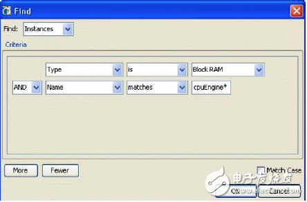
Figure 10-76 Finding Condition Settings
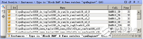
Figure 10-77 Finding results
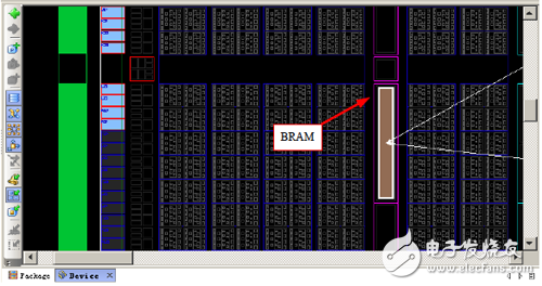
Figure 10-78 BRAM Position Constraint
In this way, you can specify the position of elements such as BUFG, DCM, Port, PPC, and MGT in the design. The position constraint created here is a fixed constraint, which is written into the UCF file. It is different from the constraint exported from ISE. The constraints exported by ISE are not fixed, and the [Device] is identified by a different color.
To establish a LOC constraint, in addition to the methods described here, you can also click on the (Create BEL Constraint Mode) button to create a position-based constraint based on Slice.
Click the (Assign Instance Mode) button to create a positional constraint for the instantiated component.
Click [Edit] → [Undo] or the button to cancel the position constraint operation.
3. View the implementation results of FloorPlan.
In the main PlanAhead interface, switch to the [Floorplan – fp_usb_TIming] view, as shown in Figure 10-79. Click the [Design Runs] tab, and you can see that the Timing Score is 0 in the implementation result of impl_2, indicating that the implementation has met the timing. Claim.
![[Floorplan – fp_usb_timing] view](http://i.bosscdn.com/blog/06/21/11/4509_0.png)
Figure 10-79 [Floorplan – fp_usb_TIming] view
4. Lock the critical logic.
In FPGA design, the performance of logic modules is often uncertain. The results of multiple implementations may vary greatly. To ensure consistency of implementation, one method is to lock the location of critical logic, such as BRAM and DSP resources. Layouts often have a large impact on design performance. We can run the place and route first to produce a timing-satisfying result, and then lock the position of the BRAM and DSP in this result as a reference to guide the next place and route.
The following describes locking the BRAM and DSP locations.
In the main PlanAhead interface, switch to the [Floorplan – fp_usb_TIming] view and click the [Design Runs] tab. You can see that the Timing Score is 0 in the impl_2 implementation result, indicating that the implementation has met the timing requirements, as shown in Figure 10-79. Double-click to open the result of this implementation. Run [Edit] → [Find] and set the search conditions as shown in Figure 10-80 to find all the BRAM and DSP resources in the design.
Lithium-boron alloy is a composite material composed of a brittle Li7B6 matrix phase with a porous structure and a ductile Li filling phase. The density is 0.88±0.04g/cm3. The appearance is silver-white metal. It is extremely unstable. It is easily deteriorated when exposed to air and reacts with water. severe. Lithium-boron alloy is mainly used as anode material for lithium-based thermal batteries. It has outstanding advantages such as high specific energy, high specific power and low polarization, electrochemical potential similar to that of pure lithium, and solid state above 600℃. It is a new type of lithium-based thermal battery. The excellent negative electrode material. Compared with the currently widely used Lithium-Silicon Alloy, the unit cell assembled with the lithium-boron alloy as the negative electrode material has better performance in both the highest voltage and the discharge working time.
Shandong Huachuang Times Optoelectronics Technology Co., Ltd. , https://www.dadncell.com