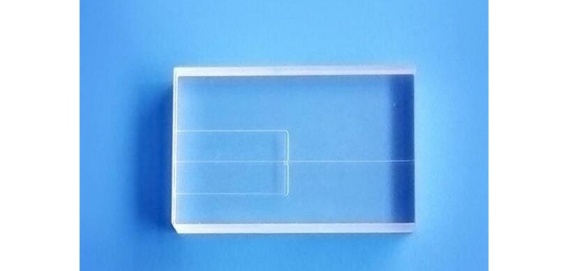
The microfluidic chip consists of a substrate (pmma; glass, pdms, etc.) and consists of channels, inlets, and detection windows. Peripheral equipment consists of peristaltic pumps, micro-injection pumps, temperature control, acceleration, and ultraviolet, spectroscopic, and fluorescent detection components. The laboratory experiment can be concentrated on a single substrate, so it is also called LABonchip. The structure of the substrate is determined by specific experiments. The design and processing of microfluidic chip substrates is the basis for microfluidic experiments. The electrical equipment attached to the chip structure is a necessary part of the chip experiment. The main functions include the flow of the driving fluid circuit, the flow direction of the fluid circuit, temperature control, image acquisition and analysis, feedback and automatic control.
Microfluidic chip production1, processing technology originated in the microelectronics industry micro-electromechanical processing technology, that is, integrated circuit chip production lithography and etching technology, micro-channel width and depth of the micron level, larger than the integrated circuit chip, but the processing accuracy requirements are
To the lower.
2. The substrate material should have good electrical insulation, heat dissipation, optical properties can be modified, can produce electroosmotic flow, can hold biological macromolecules, interfere with the detection signal little or no interference; and the working media of the chip lab There must be good chemical and biocompatibility between them and no reaction occurs. Substrate materials have evolved from silicon wafers to glass, quartz, organic polymers, and more.
3. Micron-sized structures require strict and careful control of the environment during the preparation process, including air humidity, air temperature, air and particle density in various media used in the preparation process, and are required to be completed in a clean room.
1, photolithography and etching techniques, with light glue. The mask, and the ultraviolet light are microfabricated and consist of thin film deposition, photolithography and etching.
2. Before the lithography, firstly cover the surface of the substrate with a film. Then, a photoresist is evenly covered on the surface of the film by a glue squeezing machine. The process of transferring the design pattern of the microfluidic chip on the mask to the photo-resist layer through the principle of exposure imaging is called lithography.
3. The quality of photolithography is based on the quality of the photo resist (having positive and negative points) and photolithography mask. The basic function of the mask is that the substrate produces different light absorption and transmission capabilities in the graphics area and the non-graphic area when the substrate is irradiated with a light beam (such as ultraviolet light).
The microfluidic chip is a hot area in the development of the current micro total analysis system. The purpose of its application is to realize the ultimate goal of the micro total analysis system, a one-chip laboratory, and the current key application area is the life science field.
Pros and Cons of Microfluidic Chip Materials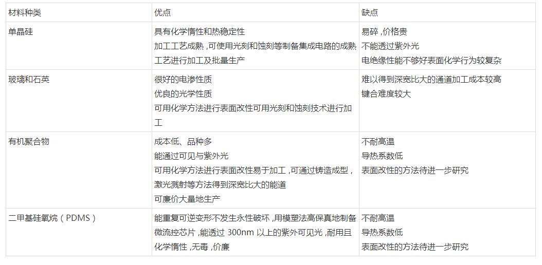
(1) Because of the good elasticity of PDMS, during the demoulding process, the processed PDMS microchannels can be easily peeled off while keeping the mold intact, thereby realizing the reuse of the mold.
(2) PDMS is flexible and easy to adsorb on substrates of other materials, and PDMS is in close contact with relatively rough surfaces. After processing, the sealing effect with the substrate is good, and the bonding process is simple.
Single, casting PDMS structure has a higher molding quality.
(3) The electrical insulation of PDMS is also very good, so it is applied to the production of various mainstream capillary electrophoresis chips; PDMS is also very insensitive to temperature and chemical inertness, and will not react with most of the liquids to be tested. Therefore, it has high biological compatibility and meets the requirements of a large number of different biological experiments.
(4) To date, microfluidic chips with PDMS as the main processing material have been widely used in medicine and life sciences.
1, with plastic: open scale called glue. A glue: B glue = 10:1. The greater the ratio of A glue to B glue, the softer the glue that comes out.
2. Homogenize: Open the vacuum deaeration mixer and put it into a weighed gel. Vacuum the glue to mix.
3. Modification: Put the processed silicon wafer into the volatilization tank, and drip 1~2 drops of modifier (methylchlorosilane) for about 3min.
4, pouring plastic: foil flattened in the dish, into the wafer mold, the wafer is lightly compacted after the plastic, be sure to make the silicone glue on the bubble-free.
5, drying: 85*C thermostatic drying oven for about 30min.
6. Stripping: After slightly cooling, remove the foil and separate the solidified PDMS from the wafer. Be careful to remove the PDMS. Be careful not to damage the wafer.
7. Cutting: Use a cutting knife to carefully cut along the outer frame of the chip, and pay attention to the neat cutting.
8. Drilling: Punching with a hole puncher, paying attention to the hole punching position and hole size.
9, clean: clean the chip.
10, microscopic examination: Use a microscope to observe whether the chip channel is qualified.
We make OBD connector with terminal by ourselves, soldering type and crimping type are both available. Also 12V and 24V type. OBD1, OB2, J1939, J1708, J1962, etc. Also molded by different type, straight type or right-angle type. The OBD connector cables used for Audi, Honda, Toyota, BWM, etc. We have wide range of materials source , also we can support customers to make a customized one to replace the original ones.
Vehicle Diagnostic Cables,Diagnostic OBD Cable,OBD2 Splitter Y Cables,OBD2 Diagnostic Adapters,OBD Heavy Vehicle Cables
ETOP WIREHARNESS LIMITED , https://www.wireharness-assembling.com