1. Select component package
When drawing a schematic, you should consider the component package and pad pattern decisions you need to make during the layout phase. The following gives some suggestions for consideration when selecting components based on component packages.
The package includes the electrical pad connections and mechanical dimensions (X, Y, and Z) of the component, that is, the outline of the component body and the pins that connect the PCB. When selecting components, consider any mounting or packaging restrictions that may exist on the top and bottom layers of the final PCB.
Some components (for example, polar capacitors) may have high headroom limitations and need to be considered during component selection. When you first start designing, you can first draw a basic circuit board shape and then place some large or position-critical components (such as connectors) that you plan to use.
In this way, you can visually and quickly see (without routing) board virtual perspectives, and give relatively accurate board and component relative positioning and component height. This will help ensure that the PCB is properly placed in the outer packaging (plastics, chassis, chassis, etc.) after assembly. You can view the entire board by calling 3D preview mode from the Tools menu.
The pad pattern shows the actual pad or via shape of the soldered device on the PCB. These copper patterns on the PCB also contain some basic shape information. The size of the land pattern needs to be correct to ensure proper soldering and to ensure the correct mechanical and thermal integrity of the connected components.

When designing a PCB layout, you need to consider how the board will be made, or if the solder is hand soldered, how the pads will be soldered. Reflow soldering (flux melting in a controlled high temperature furnace) can handle a wide variety of surface mount devices (SMDs). Wave soldering is typically used to solder the reverse side of a circuit board to secure through-hole devices, but it can also handle some surface-mount components placed on the back of the PCB.
When this technique is commonly used, the underlying surface-mount devices must be arranged in a particular direction, and in order to accommodate this type of soldering, the pads may need to be modified.
The choice of components can be changed throughout the design process. Early in the design process, it is determined which devices should use plated-through holes (PTH) and which should be surface-mount technology (SMT) to help the overall planning of the PCB. Factors to consider include device cost, availability, device area density, and power consumption.
From a manufacturing perspective, surface-mount devices are generally less expensive than through-hole devices, and generally have higher availability. For small and medium-sized prototype projects, it is best to use larger surface-mount devices or via-hole devices, which not only facilitates manual soldering but also facilitates better connection of pads and signals during troubleshooting and debugging.
If there is no existing package in the database, a custom package is generally created in the tool.
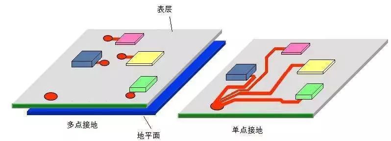
2. Good grounding
Make sure the design has enough bypass capacitance and ground plane. When using an integrated circuit, make sure to use a suitable decoupling capacitor near the power supply end to ground (preferably the ground plane). The proper capacitance of the capacitor depends on the application, capacitance technology, and operating frequency. When bypass capacitors are placed between the power and ground pins and placed close to the correct IC pins, the circuit's electromagnetic compatibility and susceptibility can be optimized.
3. Allocate the virtual component package
Print a bill of materials (BOM) for checking virtual components. Virtual components do not have related packages and are not passed to the layout stage. Create a bill of materials and view all the virtual components in the design.
The only entries should be power and ground signals, because they are considered as virtual components and are only processed in the schematic environment and are not transmitted to the layout design. Unless for simulation purposes, the components shown in the virtual part should be replaced with components that have a package.
4. Complete material data list
Check the material list report for sufficient data. After creating a bill of material report, a careful review is performed to complete the incomplete device, supplier or manufacturer information in all component entries.
5. Check for excess gates
In general, all redundant door inputs should have signal connections to avoid hanging the input. Make sure that you check all redundant or missing gates and that all non-wired inputs are fully connected. In some cases, if the input is in a floating state, the entire system will not work properly. Take the dual op amps that are often used in design.
If only one of the two op amp IC components uses one op amp, it is recommended to either use another op amp or ground the input of the unused op amp and place a suitable unit gain (or other gain). Feedback network to ensure that the entire component works properly.
In some cases, ICs with floating pins may not operate within the specifications. Typically only when the IC device or other gates in the same device are not operating in saturation—the input or output is close to or on the component supply rail—this IC can only meet the specification requirements when it operates. Simulation usually cannot catch this situation because simulation models generally do not connect multiple parts of the IC together to model floating connection effects.
ZGAR Vape Device 5.0
ZGAR electronic cigarette uses high-tech R&D, food grade disposable pod device and high-quality raw material. All package designs are Original IP. Our designer team is from Hong Kong. We have very high requirements for product quality, flavors taste and packaging design. The E-liquid is imported, materials are food grade, and assembly plant is medical-grade dust-free workshops.
From production to packaging, the whole system of tracking, efficient and orderly process, achieving daily efficient output. We pay attention to the details of each process control. The first class dust-free production workshop has passed the GMP food and drug production standard certification, ensuring quality and safety. We choose the products with a traceability system, which can not only effectively track and trace all kinds of data, but also ensure good product quality.
We offer best price, high quality Vape Device, E-Cigarette Vape Pen, Disposable Device Vape,Vape Pen Atomizer, Electronic cigarette to all over the world.
Much Better Vaping Experience!


E-Cigarette Vape Pen,Disposable Device Vape,Vape Pen Atomizer,Latest Disposable E-Cigarette OEM vape pen,OEM electronic cigarette
ZGAR INTERNATIONAL(HK)CO., LIMITED , https://www.zgarette.com