Introduction
With the popularity of automotive start-stop technology (automatically shut down the engine in idle state), more and more in-vehicle systems are required to operate at lower input voltages, and low-voltage inputs often occur at hot start (battery voltage below 6V) or cold Start (battery voltage below 3V). Figure 1 shows a common automotive system power architecture solution.
In some Power Supply systems with a mains supply of 3.3V, the front end uses a low dropout buck converter to meet the requirements (CASE 1). When needed, a boost converter can be selected to boost 3.3V to 5V (for example, to a CAN bus transceiver) or higher (CASE2). Some systems use a 5V or higher voltage supply. In this case, a “pre-boost†is required at the front end to ensure that the input voltage of the buck is not lower than the specified voltage (CASE 3). This design is applicable to the latter.
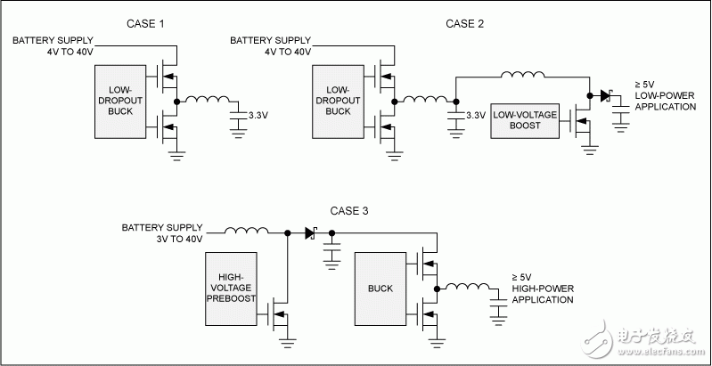
Figure 1. Automotive power plan.
In automotive design, low electromagnetic radiation is also an important indicator of performance, especially in sensitive AM bands. In this design, the switching frequency of the power supply is much higher than the AM frequency band (for example, the switching frequency is above 1.71MHz and is located at the high end of the MW band), thereby solving the interference problem. Higher switching frequencies also help reduce system size and reduce the cost of peripheral components.
Figure 2 is a schematic diagram of the switching power supply. The MAX15005 boost controller is combined with the MAX16952 buck controller to provide a reasonable on-board system power supply solution with peripheral circuits. Both ICs are synchronized to an external 2MHz clock provided by the control processor or dedicated IC to optimize the switching frequency of the power supply. The MAX15005 does not operate under normal battery conditions and provides a stable 8V OUTB voltage through the MAX16952. At cold start, as the battery voltage drops, the voltage at node OUTA is boosted by the MAX15005, ensuring that the MAX16952 provides a stable 8V OUTB voltage. The high reliability of the two ICs can meet the load dump of up to 40V in automotive environments. The program has been tested to provide up to 20W of output power () at the OUTB node. Replace the peripheral circuit to obtain higher output power.
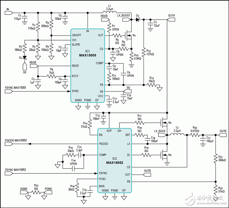
Figure 2. Schematic of the switching power supply.
Peripheral components of the MAX16952
1, output voltage and switching frequency
In order to obtain a stable 8V output at OUTB, a reasonable selection of feedback divider resistors (R22 and R21) is required. Select R22 = 51KΩ (MAX16952 data sheet recommended low side resistance R22 < 100kΩ), R21 is calculated according to the following formula:
 (Formula 1)
Where VFB = 1V (typical).
Select the standard resistance R22 = 360kΩ, the typical output voltage is:
![]() (Formula 2)
(Formula 2)
Assuming a resistance error of 1%, the minimum and maximum OUTB output voltages are:
![]() (Formula 3)
(Formula 3)
![]() (Formula 4)
(Formula 4)
Among them, VFB(MIN) = 0.985V, VFB(MAX) = 1.015V.
As recommended in the data sheet, the external clock frequency must be 1.1 times higher than the MAX16952 internal clock frequency. Since we use a 2MHz external clock to synchronize the switching frequency of the MAX16952, we must properly select the internal oscillator impedance R16 to control the internal switching frequency of "1.8MHz. In this design, R16 is chosen to be 30kΩ. To ensure that the MAX16952 switching frequency is fixed at 2MHz, voltage drops must be avoided. The MAX16952 avoids voltage drops only when the off time (tOFF) is 100ns (typ), which means the system cannot exceed the maximum duty cycle:
![]() (Formula 5)
(Formula 5)
Considering that the efficiency of the buck converter is 90%, the minimum input voltage (OUTA) that guarantees a fixed switching frequency of 2MHz is:
![]() (Formula 6)
(Formula 6)
This means that the OUTA voltage cannot be below the 11.11V threshold. To ensure that the OUTA voltage is always higher than 11.11V, when the battery voltage (IN node) is lower than 11.5V, it is necessary to turn on the MAX15005 (taking into account the L1, D2 Schottky diode voltage drop, leaving a margin of about 390mV).
When the 40V load peak voltage is reached, OUTA reaches its high voltage point, and the MAX16952 must stabilize the output voltage at 8V. Therefore, during a load dump, the duty cycle of the MAX16952 is:
![]() (Formula 7)
(Formula 7)
The MAX16952 has a minimum turn-on time (tON) of 80ns, so the minimum duty cycle (at 2MHz switching frequency) is:
![]() (Equation 8)
(Equation 8)
The 0.16 minimum duty cycle ensures a stable 8V output under load-dump conditions (up to 40V input voltage).
2, inductance and current detection
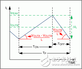
Figure 3. MAX16952 inductor current.
The use of large inductors reduces the peak inductor current and improves the efficiency of the buck converter; however, it also takes up a larger board (PCB) area and reduces load regulation. An acceptable compromise is to choose the appropriate inductance value so that LIR (the ratio of the peak-to-peak value of the inductor AC current to the average DC current) is ≤ 0.3. Based on Figure 3, use the following formula:
![]() (Equation 9)
(Equation 9)
![]() (Formula 10)
(Formula 10)
![]() (Formula 11)
(Formula 11)
According to the above equations, the inductance calculation formula can be obtained:
![]() (Formula 12)
(Formula 12)
Thus, under normal conditions (OUTA = 12V), the minimum inductance value that satisfies LIR ≤ 0.3 is:
![]() (Expression 13)
(Expression 13)
Select the standard inductor L2 = 2.2μH, LIR = 0.24, and the inductor peak current is:
![]() (Expression 14)
(Expression 14)
When the voltage of the current-sense resistor R20 reaches 68mV (minimum value), the upper current limit is reached. In order to reserve a certain margin, when the current-sense resistor is selected, the inductor current should reach the peak value (IPEAK), and the voltage drop of the current-sense resistor is 60% of the current threshold:
![]() (Equation 15)
(Equation 15)
R20 is selected as a 15mΩ standard resistor.
ZhenHuan`s line of Li-Ion Battery Charger range in output power from 6 W to 100 W features high energy efficiency and reliability, with quick charging function for 18650 batteries and li-ion batteries, etc. Our ac to dc power charger adopts constant voltage and constant current mode and accepts wall plug-in and desktop versions, all available with 2 colors LED indicator for charging status(Green and Red light). ZhenHuan`s power charger adapters solutions also includes class I and class II installations, equipped with three standard AC inlet options and different kinds of AC plugs.
Lithium Ion Battery Charger,Universal Laptop Charger,18650 Battery Charger,Li-Ion Battery Charger,UL Battery Charger,12V Battery Charger
Shenzhenshi Zhenhuan Electronic Co Ltd , https://www.szzhpower.com