1 Introduction
Power carrier communication is a unique and basic communication method for power systems. It refers to a technology that uses an existing power line to transmit analog or digital signals at high speed through a carrier. Since the widely used power line is used as the communication channel, no special maintenance channel is required, and the engineering cost is greatly reduced. This technology is widely used in street lighting control, power line security, harsh environment communication, etc., which require long distance and multi-node. However, due to the complexity and diversity of the domestic power grid, for example, when the residential power consumption peaks, a large number of loads are continuously connected and disconnected, which will cause different degrees of attenuation and interference to the carrier signal; when the carrier signal is modulated on the power line At the peak point of each AC cycle, the generated fixed pulse is very easy to lose the signal; and the existing power carrier module is expensive, and requires high-performance MCU support. Therefore, the power carrier needs a lot of research to achieve a wider application [1~2].
The purpose of this paper is to use the FSK modulation technology to realize power carrier communication, optimize the algorithm, provide a function interface, make the power carrier communication easier to use, and ensure the accuracy of communication data transmission is above 96%.
2 system overall design structure
The main function of the system is to realize that the upper computer sends data to the single-chip microcomputer through the serial port, and the single-chip microcomputer modulates the signal by FSK frequency modulation mode, and the carrier signal is coupled to the power line for signal transmission through the push-pull output circuit. At the other node of the power line, the carrier signal is restored to the original signal through the detection input circuit, the power amplifier circuit and the software algorithm, and after verification, it is sent to another host computer through the serial port. Both the signal output and the input provide a functional interface for subsequent development of user engineering [3].
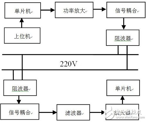
Figure 1 System overall design structure
3 system overall software design
3.1 System overall software flow chart
When the MCU starts running, after each timer, I\O port and system clock are initialized, it will wait for 5s, then detect the corresponding baud rate selection I\O port and power carrier mode select I\O port, complete all Initialization. After the program starts normal operation, the MCU will continuously receive the serial port signal and the power carrier signal, and will forward the signal after receiving the signal check.
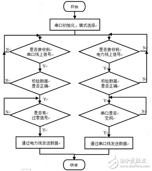
Figure 2 system overall software flow chart
3.2 Selection of power carrier mode
However, the zero mode is mainly used in the DC or no-voltage state, and the zero-crossing mode is mainly used in the AC state. Since the AC power used by the residents is 50 Hz, that is, in each cycle, there will be a peak-to-peak value and a peak-to-valley value. These two peaks have two large pulse interferences for the carrier communication transmission, that is, the power line. There is a fixed 100 Hz pulse interference. In addition, pulse interference such as 200 Hz or 300 Hz may occur in each harmonic. It is precisely because of these fixed interferences that the system must select power carrier communication when the voltage crosses zero in the AC state, that is, the voltage of each harmonic is zero at the zero crossing point, thus avoiding the interference of fixed pulses. To ensure the accuracy of data transmission [4].
As shown in FIG. 3 below, in the zero-crossing mode, a 50 Hz trigger pulse is generated by the function signal generator, and when the host computer transmits data 0xaa in a cycle of 10 ms, the output terminal of the signal coupling is detected. The carrier signal will be transmitted every time the zero crossing occurs. When the zero crossing is not successfully detected, the transmission will continue until the next zero crossing is detected again. Each time a byte of data is transferred, plus the check digit and the start bit, the time of each transfer is about 1 ms.
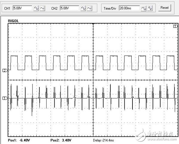
Figure 3 Actual measurement chart of zero-crossing mode
3.3 Using FSK to transmit carrier signals
In order to make the carrier signal transmission process have better anti-noise and anti-attenuation performance, FSK (Frequency-shift keying) digital modulation technology is adopted. The carrier frequency of 100k and 120k is provided by the single-chip PWM module, which makes the signal switching more convenient.
FSK frequency modulation technology, that is, binary frequency shift keying, is switched by the frequency of the carrier signal with constant amplitude as the input code stream changes (called treble and bass, representing binary 0 and 1). In this system, a carrier frequency of 120k represents a carrier frequency of 0,100k representing 1. In order to reduce the discontinuity of the phase between each signal switching, and send enough signals at the same time for the acquisition of the detection input, the transmission time of each bit signal is selected to be 100 ms. That is, 12 square waves will be sent at 120k, and 10 square waves will be sent at 100k, so there will be no extra waveform between the switching between 1 and 0.
Since there is a large capacitance on the side of the power line, a bit of 0 is sent as a start bit before each power line transmission. Otherwise, the first bit of data coupling is susceptible to the charge and discharge of the capacitor, and there is a large error.
3.4 Collecting carrier signals by multiple comparison methods
When the timer of the MCU collects the first signal input, an interrupt is generated, and the 100ms timer is turned on, the value of the current interrupt timer is recorded, and the signal is continuously collected. The interrupt timer is turned off until seven interrupts are acquired. Calculate the number of clocks between each interrupt, that is, calculate the frequency of the signal. When it is around 100 kHz, the flag of 1 is incremented by 1. When it is around 120 kHz, the flag of 0 is incremented by one, and finally the bit is judged. Value. When the 100ms timer overflows, the interrupt timer is restarted and the next bit of data is accepted until all data reception is completed. If the interrupt timer has not been interrupted for 100ms until it overflows, the received data is cleared and the signal input is re-waited.
Long lifetime and durability: based on the LED technology & the new structure, so that this lamp can reach 100,000 hours of long life in any case. Relative to the glass neon tube, its durability, because at all there is no need to consider the problem of broken glass.
Outdoor Business Signs,Custom Led Signs Outdoor,Outdoor Lighted Letters,Outdoor Neon Bar Signs
Shenzhen Oleda Technology Co.,Ltd , https://www.baiyangsign.com