Why is heat dissipation important? For most semiconductor applications, quickly transferring die heat and dissipating heat to a larger system prevents areas of high concentration of heat on the silicon.
This article refers to the address: http://
Typical operating temperatures for silicon dies range from 105 ° C to 150 ° C, depending on the application. At higher temperatures, the metal diffuses more and more, and eventually the device will fail due to a short circuit.
The reliability of the die is highly dependent on the time the die is in a high temperature environment. In a very short period of time, silicon dies can withstand temperatures well above the published acceptable values. However, the reliability of the device will be affected over time.
Thermal modeling has become an important tool in the automotive industry due to this delicate balance between power demand and heat limit. The automotive safety industry is now pursuing smaller components and fewer components, forcing semiconductor suppliers to consume more power in exchange for integrating more functionality into the chip.
The resulting higher temperatures will ultimately affect reliability, which in turn affects vehicle safety. But by optimizing die layout and power pulse timing early in the design cycle, design engineers can further optimize development cycles by providing optimized designs with fewer silicon testers.
Semiconductor thermal packaging
The automotive electronics industry uses a variety of different semiconductor package types, from small single-function transistors to complex power packages, which provide more than 100 leads and specially designed heat dissipation.
The role of the semiconductor package is to protect the die and provide electrical connections and thermal management between the device and external passive components in the system. This section will focus on the performance of semiconductor packages in terms of die heat dissipation.
In a leaded package, the die is mounted on a metal disk called a die pad. This pad supports the die throughout the manufacturing process and provides a good thermal conductive surface. A common type of semiconductor package in the automotive industry is an exposed pad, or a PowerPAD type package (Figure 1).
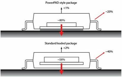
The bottom of the die pad is exposed and soldered directly to the PCB to provide direct heat transfer from the die to the PCB. The main heat dissipation path goes down through the exposed pad soldered to the board so that heat can be dissipated through the PCB to the surrounding environment.
The exposed pad type package conducts approximately 80% of the heat to the PCB through the bottom of the package, leaving 20% ​​of the heat dissipated from the device pins and package sides. The heat dissipated from the top of the package is less than 1%.
The non-exposed pad package is a similar leaded package (Figure 1). In this package, the plastic is completely filled around the die pad, so there is no direct thermal path to the PCB. About 58% of the heat is dissipated from the leads and the sides of the package, 40% of the heat is dissipated from the bottom of the package, and the heat dissipated at the top accounts for about 2%.
Heat can be dissipated by conduction, convection or radiation. For automotive semiconductor packages, the primary way to dissipate heat is by convection conduction to the PCB and ambient air. Even with the presence of radiation, only a small amount of heat can be dissipated.
Thermal challenge
Automotive systems that operate normally, safely and comfort are highly dependent on semiconductor products. Today, semiconductor products are found everywhere in body electronics, airbags, thermostats, radios, directional control, passive access control, anti-theft systems, and tire pressure monitoring systems.
Despite the emergence of many new applications in the automotive semiconductor industry, the three traditional areas still maintain independent environmental requirements: the interior of the cabin, the dashboard front panel and the engine compartment. In general, there are three major factors that continue to challenge the automotive environment: high ambient temperatures, high power, and limited material thermal properties.
The temperature in the automotive environment is very different from that in other environments. In general, consumer electronics have an operating temperature of around 25 ° C and an upper limit of about 70 ° C. On the other hand, electronics in automotive passenger compartment or instrument panel applications will operate at high temperatures up to 85 ° C (see attached table).
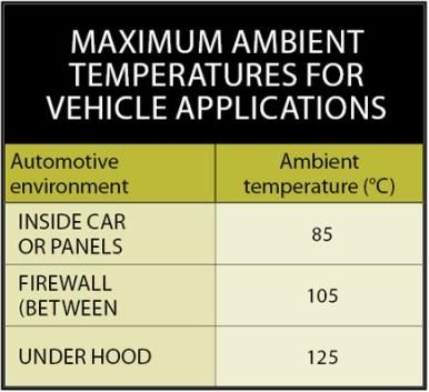
In dash panel applications, electronics are located between the engine compartment and the car compartment, and the device may be exposed to ambient temperatures up to 105 °C. Engine compartment applications need to operate at ambient temperatures up to 125 °C.
Thermal considerations are particularly important in safety-related systems such as power steering, airbags, and anti-lock braking systems. In brake and airbag applications, the power level is likely to be as high as 100W in a short time (1ms).
The ever-increasing functional requirements and the numerous resources of integration drive the power of the die. The die temperature of some automotive semiconductors can be as high as 175 ° C to 185 ° C in a short time. This temperature is typically a thermal shutdown threshold for automotive devices.
As more safety features increase, the heat dissipation requirements are also increasing. Although airbags have been common in automobiles for more than a decade, some cars now have as many as 12 airbags. In actual deployments, multiple airbags require sequential operation, thus creating a much more difficult thermal design challenge than a single conventional airbag.
It is no secret that the cost of automotive components is as low as possible for the thermal challenges of material properties. Plastic materials are replacing a large number of metal modules and PCB housings. Plastic housings have the advantage of lower production costs and are lighter in weight. However, corresponding to lower cost and lighter weight, the heat dissipation performance is lowered.
Plastic raw materials have very low thermal conductivity, in the range of about 0.3 to 1 W/mK, so they are essentially thermal insulators. Undoubtedly, changing to a plastic case will hinder the heat dissipation of the system and increase the thermal load of the semiconductor device.
Why modeling?
In the automotive semiconductor industry, modeling efforts focus on the thermal performance and design of individual devices. It is generally considered that careful modeling can be used to obtain modeling data.
System-level simplification (such as removing unrelated low-power devices from the model) can be simplified to simplify the thermal model for fast modeling by using simplified rather than detailed PCB copper routing, or assuming the chassis is dissipated at a fixed temperature. In addition, these simplifications still accurately reproduce the thermal resistance network.
Package-level thermal modeling can be used to evaluate potential package design changes without the need for costly development and testing, eliminating the need for material construction. The semiconductor package design can be changed according to the application requirements to achieve the best heat dissipation.
With an exposed pad package like PowerPAD, heat can be quickly dissipated from the die to the PCB. Larger die pads, better connections to the PCB, or improved die pad design can improve device thermal performance.
Thermal modeling techniques can also be used to examine the effects of potential material changes in the device. The thermal conductivity of the encapsulating material varies widely, from as low as 0.4 W/mK (thermal insulator) to over 300 W/mK (good thermal conductor). Using thermal modeling techniques helps balance the relationship between product cost and performance.
Modeling verification
For critical systems, careful laboratory analysis can determine thermal performance and operating temperature. However, laboratory measurements of these systems are time consuming and costly. At this point, thermal modeling technology is a powerful tool to help solve system cooling needs and meet operational requirements.
In the semiconductor industry, thermal modeling has become an early part of the concept test and silicon die design process. The ideal thermal modeling process began months before manufacturing the die. IC design engineers and thermal analysis engineers will evaluate the die layout and power consumption of the device.
The thermal modeling engineer then creates a thermal model based on the results of the above assessment. Once the thermal model is built, the design engineer and modeling engineer will review the data and adjust the model to accurately reflect the likely application scenarios.
All finite element analysis (FEA) modeling validation is highly recommended. TI's strategy is to conduct correlation studies that compare thermal modeling results with physical measurements of the system.
These correlation studies can highlight multiple potentially erroneous areas, including material properties, power definitions, and layout simplification. Although no model can perfectly replicate a real system, the assumptions made during the modeling process must be carefully considered to ensure the most accurate system description.
In terms of material properties, published values ​​generally indicate the overall thermal conductivity of a particular material. However, thin layer materials are often used in semiconductor applications, and increased surface area of ​​the material will result in a decrease in thermal conductivity (relatively the same volume value).
Pay particular attention to the power consumption described in the model because the input power of the device is constantly changing over time during operation. Power consumption on the board or elsewhere in the system can also affect the true power consumption of the die surface.
Modeling type
There are currently four major thermal models available for semiconductor package design: system level, package level, die level, and die level transient analysis. In automotive semiconductors, system-level thermal modeling is especially important because it illustrates how a particular device will operate in a particular system.
In general, thermal modeling of automotive semiconductors takes PCB into account because PCBs are the primary heat sink for most semiconductor packages. The various components of the PCB, including the copper layer and the thermal vias, should be added to the thermal model to accurately determine the thermal behavior analysis. In addition, all unique physical shapes should be included, such as recessed heat sinks, metal connectors such as screws or rivets.
Forced air flow around the system and PCB also plays an important role in system convection heat dissipation. Often the thermal modeling object in the semiconductor industry is a single high power device. However, other power devices on the PCB also have a large impact on the overall performance of the system.
Simplifying the input of these packages while still maintaining a certain level of accuracy usually requires a compact model. A compact model is a less complex thermal resistance network that provides a reasonable approximation of the thermal performance of these non-critical devices.
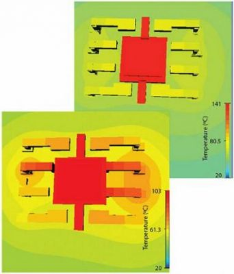
In smaller devices with fewer pin counts, other methods can be used to improve thermal performance (Figure 2). For example, melting multiple package leads onto the die pad of the device can greatly improve the overall junction temperature without affecting device operation.
Modeling assumption
Die-level thermal analysis begins with an accurate description of the silicon die layout, including all power-consuming areas on the die. In the simple case, it is assumed that the power is evenly distributed on the silicon wafer.
However, the power distribution of most die layouts across the die is not uniform, depending on the functionality. This uneven power distribution is critical to the overall thermal performance of the device. For devices that require good heat dissipation, more attention needs to be paid to the power structure distribution on the die.
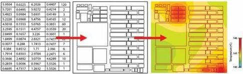
In some thermal analysis software programs, the die layout can be entered using a comma-separated variable (.csv) input format (Figure 3). This makes it easy to transfer information between die layout and thermal modeling software. Depending on the complexity and power level of the device, these power-consuming areas on the die may vary from two to three to several hundred.
Thermal modeling engineers should work closely with IC design engineers to determine the area of ​​power consumption that needs to be included in the thermal model. In general, some small areas with very low power consumption can form larger areas, simplifying the thermal model while still representing the overall power consumption of the device. Similarly, in the thermal model, background power or static power can be used across the entire die surface to represent most of the power in a non-critical low-power die structure.
Some device features often require small areas on the die to provide greater power. These high power areas may cause local hot spots, and the temperature of these hot spots may be much higher than the surrounding silicon.
Thermal modeling helps to highlight thermal issues, such as where the clusters of medium power silicon products are located very close together that can cause residual heat and may cause thermal stress on the die to be evaluated.
The model also facilitates the placement or calibration of embedded thermal sensors on the die. Ideally, the temperature sensor should be placed at the center of the highest power consumption area on the die. However, due to the constraints of the layout, it is often impossible to achieve. When placed away from the center of the high-power area, the temperature sensor will not be able to read the exact maximum device temperature.
The thermal model can be used to determine the thermal gradient across the die, including the thermal gradient of the sensor location. The sensor is then calibrated to derive the temperature difference between the hottest zone and the sensor location.
The above models assume a constant DC power input. However, in actual operation, device power varies with time and configurability. If the thermal system is designed for only the worst case power consumption, the thermal load may become unusable.
There are many ways to evaluate transient thermal response. The easiest way is to assume a DC power supply on the die and then track the thermal response of the device over time. Another method is to input a varying power supply and then use thermal analysis software to determine the final steady state temperature.
The third and most useful transient modeling is to observe the "time response" of the varying power supply at multiple die locations (Figure 4). This method can be used to capture interactions between devices that may not be apparent under normal conditions. Transient modeling also helps to observe the entire process of die operation that is different from normal device functions, such as the power-up or power-down mode of the device.
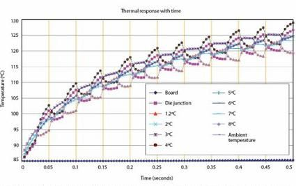
In many automotive systems, such as brake actuation or airbag opening, device power is maintained at a low level for most of its life. During the start-up of the airbag system, the energy pulse can reach a very high value in a short time.
Performance improvement
Design optimization and lower overall temperature are the thermal modeling goals of the automotive semiconductor industry. Reducing the die junction temperature during operation can improve device reliability.
Minor improvements in system, board, package or die performance can significantly improve final temperature performance. However, device and system limitations may stifle some of these recommendations.
Methods to improve thermal performance include air flow, heat transfer paths, or external heat sinks. Another approach is to provide more metal area for heat dissipation, such as adding external heat sinks, metal connections to the base, PCBs with more layers or higher density copper layers, thermally conductive copper plates, and thermal vias.
Thermal vias located below the exposed paddles of the device help to quickly dissipate heat from the device and speed up the dissipation of heat to other parts of the board. Semiconductor device packages are designed to quickly dissipate heat from the die to larger systems.
Using higher thermal conductivity materials, directly connecting the PCB like PowerPAD, melting leads to the die pad or mounting external heat sinks can help improve the thermal performance of the semiconductor package. The semiconductor die itself allows for a variety of ways to minimize the overall temperature. Of course, the best way to reduce temperature is to reduce power consumption.
For silicon circuit design and layout, good heat dissipation methods include a larger heat dissipation area, making the power consumption area away from the die edge, using a long and narrow power consumption area instead of a square area, and providing sufficient space in a high power consumption area. Wait. Silicon is a good thermal conductor with a thermal conductivity of approximately 117 W/mK. Using the maximum amount of silicon around the power consuming area increases the heat dissipation of the device.
For transient power dissipation on the die, staggering the power pulse to reduce transient power will reduce the overall temperature. This creates a longer delay between the energy pulses for heat dissipation or for sharing high power events across multiple areas on the die. These transient changes allow the thermal system to recover before more heat is applied. By carefully designing the die, package, PCB, and system, the thermal performance of the device can be significantly improved.
DIM to warm spot led/DIM To Warm led Spot Light to use light-emitting diodes as a light source for lighting. Use more traditional halogen spotlights, low luminous efficiency, more power, increased by exposure to ambient temperature, short life. DIM To Warm led Spot Light source on the light emitting principle, energy saving, environmental protection level is far superior to traditional lighting. And the formation of unidirectional LED glowing light distribution for lighting the perfect support.
Currently LED as light source lamps made more and more, DIM To Warm Led Spot Light is one of the most acclaimed LED spotlights, as compared with other LED lamps, LED spotlights lower prices.


1. DIM To Warm led Spot Light can be driven using a low voltage DC,like led par30,led par38: a load of small, weak interference advantages of the use of environmental requirements are lower.
2. DIM To Warm led Spot Light can better control the spectral composition of light emission, which can be good for museums and galleries in the local or accent lighting.
3. LED lighting luminous point is very strong: light attenuation is much lower than traditional light sources, LED lighting prices civilians. 4. LED spotlights response time is very fast: in the microsecond level, as long as the switch is opened, will be bright, no delay and flicker.
5. DIM To Warm led Spot Light highly concentrated light energy emitted: concentrated in a smaller wavelength window, high purity.
6. A very long life: generally between 50 000 -10 million hours, because LED is a semiconductor device, even frequent switching, will not affect the service life.
DIM To Warm led Spot Light Application:

Mingxue Optoelectronics Co.,Ltd. has apply the I S O 9 0 0 1: 2 0 0 8 international quality management system certificate, For DIM To Warm led Spot Light we apply the CE, RoHS and SAA certificate for our led lighting product.


DIM To Warm led Spot Light
Dim To Warm Spot Light,White Dim To Warm Spot Light,Dim Warm Spot,Led Dim To Warm
Shenzhen Mingxue Optoelectronics CO.,Ltd , https://www.mingxueled.com