Zhang Wei, Wang Shicheng, Wang Weiming, North China Institute of Computing Technology
Keywords: VPX bus; "Godson"; domestic computer module; computer module design
0 Preface
VPX is a new-generation industrial bus standard based on the VITA 46 (VME Bus International Trade Association) protocol, which was upgraded from the original VME (VersaModule Eurocard) bus system and is compatible with XMC (VITA 42). Fiber Channel (Fibre Channel), PCI-E (Fast Peripheral Component Interconnect), Rapid IO (Rapid Interconnect Technology), HT (HyperTransport Bus) and other high-speed serial bus protocols. In 2010, the release of REDI (Enhanced Ruggedized Design Implementation, VITA48) enabled the VPX system to have both a reinforced mechanical structure and a stronger cooling capacity. These new features, coupled with the open architecture of VPX, make VPX the best choice for meeting the needs of harsh environment applications, especially for the new generation of military buses.
General-purpose CPU independently researched and developed by the Chinese Academy of Sciences — "3G" is the first product of the "Godson" No. 3 multi-core processor series. It is manufactured on 65 nm process and integrates four 64-bit superscalar general-purpose processors in a single chip. Nuclear, the highest working frequency is 1 GHz. Its interfaces mainly include HT interface, DDR (double rate synchronous dynamic random access memory) 2/3 (memory) controller interface, LPC (low pin count) interface, serial port, SPI (serial peripheral interface), JTAG (Joint Test Behavior Organization) interface, EJTAG (Enhanced JTAG) interface, and system control interface.
In this system, the latest VPX bus standard and localized CPU are combined to develop a dual "Loongson" 3A computer module based on the VPX standard, and applied to a VPX chassis with a reinforcement feature. After passing the test, it has been Delivered to users. The following describes in detail the two aspects of the computer module design and testing.
1 Domestic computer module design
1.1 Principle Design of Computer Modules
As the design of computer modules is to incorporate the VPX standard, the design can be divided into three major parts: The first part is the calculation processing part consistent with the universal main board, including the processor, North-South bridge, memory, B10S (Basic Input Output System) , memory, Ethernet controller, and power and clock; the second part is the IPMI (Intelligent Platform Management Interface) management part, including management controller, hot swap, power management, temperature detection, etc.; Part 3 is the VPX bus interface . Figure 1 focuses on the block diagram of the calculation processing section.

URAT-Universal Asynchronous Receiver Transmitter; Boot Rom-Boot Program Memory; SERDES-serializer/deserializer; MDIO-manager data input and output; VGA-video graphics array; USB-universal serial bus; SATA-serial Advanced Technology Annex; CH-channel; MC-memory controller Figure 1 Block diagram of calculation processing
As shown in Figure 1, the "Loongson" 3A contains two sets of memory controllers. The two CPUs are directly connected to the 2 Gbyte memory particles by the first set of controllers, achieving a total of 4 Gbytes of memory capacity. The "Godson" 3A contains two HT buses at the same time. The two HT buses of CPU0 are connected to the CPU1 and the North Bridge, respectively. CPU1 uses one set of HT bus and the other set is empty. The two CPUs connect to the BIOS chip through the I PC interface and provide serial output. During the actual operation, only the BIOS chip connected to CPU0 provides the loaded information after power-on, and the boot information printed after power-on is checked through the serial port of CPU0 to confirm whether the CPU is operating in a normal state. If there is a problem with the work of the CPU, it can be judged by which part of the startup process a fault has occurred by printing the information to stop the output or an infinitely repeated position, thereby performing the test and verification.
Northbridge connects 128 Mbyte of independent video memory, and outputs two kinds of display signals, DVI (Digital Video Interface) and VGA. Northbridge provides two PCI-E interfaces, one of which is a x16 PCI-E interface that can be used to expand discrete graphics cards. The other group is a six-by-one PCI-E interface, which can be composed of a single x4 and two x1 methods. The Ethernet controller can be connected to the extended network interface in the manner shown in Figure 1 and can also be composed of 3 x 2 or 6 x 1 mode expansion interfaces.
The South Bridge and the North Bridge are connected via the A-Link Express (A-Link Express II) to output low-speed signal interfaces such as USB, SATA, PCI, IDE (Electronic Integrated Driver) and LPC.
The external output of the entire module and the power supply interface are realized through VPX connectors (connectors P0 to P6). There are 7 sets of connectors on the board to communicate with the backplane. The connector P0 provides the power signal and the common layer signal, including the slot confirmation signal and the management bus signal. The remaining six sets of connectors (P1 to P6) output high-speed signals such as PCI-E bus and Gigabit Ethernet, and low-speed signals such as display and USB.
1.2 memory layout design
According to the definition of the VPX standard, the computer module needs to be implemented in the size of the Eucalyptus 6U standard. The design of the module includes more than 2,000 components, hundreds of differential signals, and more than a dozen power supplies. It has great difficulty in layout and wiring.
The memory design is a key design of the entire board, using memory particles to meet the system's reinforced seismic performance.
A single "Loongson" 3A processor integrates two DDR 2 channels. This module design includes two CPUs. Each CPU is connected to one channel of memory particles. Each channel uses eight 8-bit wide 256 Mbyte memory particles. Adding an 8 bit wide ECC (error correction code) check bit memory particle, each channel supports a capacity of 2 Gbytes, a total of 4 Gbytes for the 2 channels, and 18 memory particles. Since signal length matching is one of the key factors of timing characteristics, these 18 memory designs must comply with the following 4 design rules to work properly: 1) The length error between each differential pair in the data signal group is not greater than 10 Mil (0.254 mm), and the difference between the line length of the single-ended signal and the differential signal in the group is less than 50 mil (1.27 mm); 2) The length error of each differential pair in the clock group is not greater than 10 mil, and between groups The difference in line length is less than 100 mil (2.54 mm); 3) The length relationship between CTRL (control signal) and CLK (clock signal) must satisfy 500 mil ≤ CTRL-CLK ≤ 1000 mil; 4) Differential signal impedance is controlled at 80X (1 ± 0.1) Ω, single-ended signal impedance is controlled at 50X (1 ± 0.1) Ω.
In order to achieve the signal length requirements proposed in the above design rules, layout according to Figure 2 at design time. Around each CPU, 9 memory particles are placed on the front and back, and 5 or 4 sides are placed on each side. The dark boxes in the figure indicate the back memory locations.

Figure 2 memory layout
In the memory signal wiring design, a serpentine wiring method is generally used for length matching, and the spacing between the data signal lines should be at least 2 times the signal line width (edge ​​to edge) to reduce the crosstalk between signals. The signal line length is calculated by taking the length of the internal lead of the BGA (ball grid array package). Each additional via during routing is approximately equivalent to a 90 mil (2.286 mm) transmission line length, so it is best to control the number of vias per signal line to two.
In addition to meeting the signal line length matching requirements, it is also necessary to consider the continuity of the signal's return path and impedance, so it is best to use the complete ground plane as the reference plane for the signal. Because the general power layer will be divided into several areas, if the signal is taken as the reference plane, the signal will cause cross-segmentation problems, which will result in signal impedance discontinuity, which will directly affect the signal transmission quality.
In the actual wiring design, the above rules regarding the length of the signal line can be directly added to the setting options of the design software. When the length of the wiring does not meet the requirements, the software will automatically perform a DRC (Design Rule Check) check and light the line to facilitate the designer to modify the wiring of the signal line.
1.3 Cabling Design for Other Signals
The HT bus is also a key point in design. The module is divided into two groups of HT bus, a group of HT bus connects the communication paths between two CPUs, and the other group of HT buses is located between the main CPU and the North Bridge, which is the top of the entire board communication link. Once the HT bus is in trouble, the debugging of the whole board will be very difficult, so we need to design the HT bus signal according to the following design rules: 1) Each of the 16 pairs of HT bus transmit and receive signals, in which the receive signal is divided into 2 in sequence. Group, each group includes 8 pairs of signals and corresponding 1 pair of CTRL signals and 1 pair of CLK signals. The division rules of the transmitted signals are similar, so that a total of 4 sets of signal groups are formed; 2) the length error within the differential signals is less than 5 mils (0.127) Mm); 3) The difference in length between differential signals of the same group is not more than 100 mils and the signal interval is 20 mils (0.508 mm) or more; 4) The difference between the lengths of the signal groups is less than 1500 mi1 (38.1 mm); 5) All signal lengths of the HT bus are controlled between 1 and 8 in; 6) Impedance of the differential signal is 100×(1±0.15)Ω. In addition, similar to memory wiring, note that the same set of signals must be routed in the same layer, and the reference plane for all signals is ground-based.
The computer module also includes high-speed signals such as A Link, PCI-E, and Gigabit. These signals must be performed in accordance with the rules for high-speed signal wiring, and the signal line impedance must be strictly controlled. The differential signal impedance is generally controlled around 100Ω. SATA, USB, and other low-speed differential signals must obey their corresponding rules, otherwise they will malfunction when the hard disk reads and writes and other operations, and the response is very slow. In addition, the design should also pay attention to the analog signal traces of the display interface. They should be shielded with a 10 mil ground wire (5 mil pitch). Each ground wire should be connected to the ground plane every 750 mils (19.05 mm). Use irregular spacing between vias to ensure no interference with other digital signals.
1.4 SERDES Network Design
According to the VPX standard, the network switching link in the system is designed as a SERDES mode, ie a high-speed serial mode. SERDES is an abbreviation for Serializer/Deserializer. To send a group of parallel signals (one word) in one clock cycle, the encoder on the transmitting side converts the parallel signals into serial signal transmission. The signal receiver recovers the clock signal and data through the multi-phase sampler and decodes the original parallel signal to complete the transmission process. The SERDES signal is a backplane transmission signal. Unlike the conventional motherboard network 10 M/100 M/1000 M BASE-T, it cannot be directly connected to the network cable through an RJ45 socket. It needs to pass through the backplane and the switching chip in the switch module. Direct communication.
Based on this demand, the final selection of the Intel Corporation 82571EB design, which includes a × 4 PCI-E interface connected to the North Bridge, the output of two channels of SERDES signal to the backplane, to achieve network switching capabilities.
1.5 Computer Module Power Design
The architecture of the dual processor is used in the design, and the power consumption of the whole board is increased by about 1 times compared with the single processor board. So when designing the power supply section, in order to reduce the pressure on the power supply chip that supplies power to the 1.1 V core voltage, three identical power supply chips are selected to provide respective nuclear voltages for the two CPUs and the Northbridge, and the input voltage of the chip is 12 V, this increases the output voltage of the backplane 12 V at the same time. However, this problem can be easily solved by using a VPX connector design. Because in the VPX standard, the power output of the system design is 5 V (VS3) and 12 V (VS1, VS2), while the power supply of VS1, VS2, and VS3 can reach 22 A, that is, the maximum power corresponding to these two types of power supply respectively. Up to 110 W and 528 W. So long as the power module can provide enough power output, the VPX connector can provide the power to the computer module. Therefore, the large power supply is also the best place in this system to reflect the advantages of VPX.
2 test process and comparison
2.1 Power Test
In the whole board debugging process, the power circuit is first tested. According to the principle of the design of the 10 main power in order to measure, to ensure normal power supply. The tested output voltage of 12 V is about 3.5 A, and the output current of 5 V is about 2 A.
2.2 Functional Test
Functional testing is relatively simple, as long as the computer module can achieve normal computer functions, including display, network, USB and other parts. However, functional tests sometimes do not reflect design issues, such as memory. In the BIOS stage, after the system is powered on, the output information of the serial port will show information about the memory. It can be seen that the memory capacity is 4 Gbytes, but this is a value directly written by the software. It does not actually indicate that all the Memory particles. Because the system can start normally and guarantee basic operation, it is easy to mistakenly think that the memory has been working normally, but it is found that the system will crash during the process of copying a large amount of data files. Finally through the memory performance test to determine the memory parameter settings, you need to modify the memory parameters in the BIOS to correct this problem.
2.3 Performance Test
In order to ensure that the system can work stably and continuously, various performance tests are also required. Through testing, problems hidden in some designs can be exposed for solving, otherwise these problems may constitute instability factors of the system. For example, if the memory cabling is not in accordance with the rules, it can not be seen in the functional testing stage. The computer module can normally power on, load the operating system, and perform ordinary operations. It is only a bit slow, but it cannot be judged as a design. Which aspect of the problem occurred, then through the performance test, found that the memory read rate is low, directly affect the operation of the application, which can be solved for memory problems. Performance testing includes: CPU testing, memory testing, hard disk testing, network testing, and stability testing.
2.3.1 CPU Calculation Performance Test
The CPU test uses the open source test tool Nbench software under the Linux system. This tool can test the computing speed and memory access speed of CPU integer and floating-point data, and calculates the score according to the corresponding base, as shown in FIG. 3 .
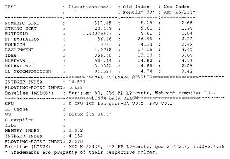
Figure 3 CPU computing performance test results screenshot
Table 1 shows the test results of CPU computing performance. By comparison, the two-way "Godson" 3A module has two CPUs working together. The test results obtained are better than those of the single-channel "Godson" 3A module, which has an even greater advantage in computational performance.

Table 1 Comparison of Single Dual CPU Module Performance
Table 2 shows the test results of the two-way module and general-purpose computer after calculating the base number. Compared with the general-purpose computer of Intel Corporation, the performance of the memory part is only in the "Pentium" 3 generations stage, the integer calculation is higher than the "Pentium" 3 generations close to the "Pentium" 4 generation level, and the floating point type The level of calculation is lower. The localized CPU “loongson†3A does have a certain gap compared with the processors commonly used at this stage.

Table 2 Comparison of overall performance test results
2.3.2 Memory Read Rate Test
The memory test uses the stressapptest software, which can specify the memory size to be tested and the test time when the command is entered. See Table 3 for the results. Compared with the single-channel "Godson" 3A computer motherboard test results, it can be seen that although the memory capacity used by both is 4 Gbytes, the memory read rate of the dual-channel module is up to twice that of the single-channel motherboard. Therefore, when the system runs various programs, the speed of the dual-channel module is significantly higher than that of the single-channel motherboard. The two-way module is limited by the size of the board and can only connect the memory in two channels. If the two CPUs can connect the memory in four channels, the performance can be greatly improved.

Table 3 Comparison of Memory Read Rate Test Results
2.3.3 Hard Disk Read/Write Speed ​​Test
The hard disk test adopts iozone software. The test command specifies that the size of the test file is increased from 1 Mbyte to 256 Mbyte, and the iozone.xls file is generated. The results obtained are divided into two parts: read speed and write speed.
Table 4 shows the test results of the read and write speed of the hard disk. By comparison, the difference between the two is not obvious. It can be seen that for the read/write control of the hard disk, the number of CPUs does not have a great influence on the number of CPUs, and its impact mainly depends on the hard disk itself.

Table 4 hard disk read and write speed test comparison
2.3.4 Network Performance Test
The network test uses the open source test tool iperf under the Linux system. It sends 110 Mbytes of data packets every second. A total of 1.07 Gbytes of data packets are sent for 10 s. The average rate of TCP (Transmission Control Protocol) connections is 919 Mbit/s. . The test shot is shown in Figure 4.
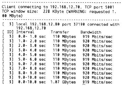
Figure 4 Network Performance Test Screenshot
2.3.5 Stability Test
The stability test uses self-developed test software to perform picture refresh and calculation at a high frequency, and then observe the CPU usage, memory usage, and the specific conditions of running various threads. The main purpose is to test the working conditions of the CPU and memory under certain pressure, whether there will be problems of crash or restart, and the general stability test must continue for more than 3 days. As shown in Figure 5, there are currently 5 groups of open test software. The occupancy rate of 8 cores of 2 CPUs is all over 97%. The used memory capacity is 3.4 Gbytes, and the running time is 57 minutes.
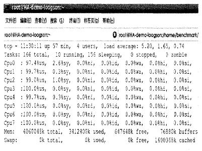
Figure 5 stability test screenshot
According to the above tests, the VPX-based dual "Loongson" 3A computer module can complete all the functions of the general-purpose motherboard and achieve the normal performance level. It can be inserted into the corresponding slot of the VPX chassis to realize localization calculation with reinforced seismic capability. platform.
3 Conclusion
The existing military reinforcement computer systems generally use foreign CPU motherboards. In the function, the localization platform computer system can be completely replaced, but there is still a certain gap in performance. However, localized CPUs and operating systems are safer and more reliable. When they are applied to military projects, they are conducive to the confidentiality of military information in China. And with the continuous improvement of the level of localization, combined with advanced bus technology, such a computing platform will inevitably become the future development trend.
Dog Training Transmitter,Vibration Training Collar,Remote Control Vibration Collar,Rechargeable Dog Shock Collar
Elite-tek Electronics Ltd , https://www.aetertek.ca