This article discusses ADI's next-generation SPI control switches and their architecture to address this design challenge, and what advantages it has in increasing channel density relative to parallel control switches. ADI's innovative multi-chip packaging process enables the new SPI-to-parallel converter chip to be combined with existing high-performance analog switch ICs in the same package. This saves space without affecting the precision switching performance.
Maximizing the number of channels in a test device is critical because the more channels there are, the more devices can be tested in parallel, compressing the test time and cost of the end customer. The tester shares its resources through switches to support multiple devices under test (DUT), so switches are a key component in increasing the number of channels. However, the more switches in parallel control, the more control lines, and the corresponding board space increases, which severely limits the channel density that can be achieved.
In this case, the use of SPI-controlled switches offers significant advantages in solution size and channel count. The SPI switches can be daisy-chained, which significantly reduces the number of digital lines required compared to traditional solutions.
This article will detail the problems encountered in the process of maximizing the number of channels, discuss the traditional methods for controlling a group of switches and their shortcomings, propose an analog switch solution for SPI control, and finally introduce the best performing ADI SPI in its class. Control the precision switch.
Frequently asked questions about maximizing the number of channelsWhen the main goal of module development is to maximize the number of channels, the board space becomes very precious. Switches are the key to increasing the number of channels in a system, but as the number of switches increases, the switches themselves, the logic, and the devices needed to generate these logic signals take up a lot of board space, reducing the available space. Ultimately, only a very limited number of channels can be achieved, subject to the relevant factors required to control the switch itself.
Traditional parallel switching solutionThe most common solution to increase channel density is to use switches controlled by parallel logic signals. This requires a lot of GPIO signals, and standard microcontrollers cannot provide so many signals. One solution to generate GPIO signals is to use a serial-to-parallel converter. These devices output parallel signals and are configured by serial protocols such as I2C and SPI.
The layout in Figure 1 shows eight ADG1412 four-channel, single-pole, single-throw (SPST) switches in a 4 x 8 cross-point configuration on a six-layer board. These switches are controlled by two serial-to-parallel converters with serial lines from a single control board. Each converter provides 16 GPIO lines that are distributed to 8 switches. The layout shows the footprint of the device, power supply decoupling capacitors, and digital control signals (gray). The 4 x 8 matrix solution with parallel control switches measures 35.6 mm x 19 mm and occupies 676.4 mm2.
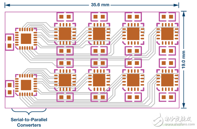
Figure 1. Parallel control switch 4 x 8 matrix layout
It is apparent from Figure 1 that a large proportion of the area is occupied by the serial to parallel converter and the digital control line, rather than being occupied by the switch itself. This inefficient use of board space is terrible, greatly reducing the number of switches in the module, which in turn affects the number of system channels.
SPI switch solutionFigure 2 shows a 4 x 8 crosspoint configuration with eight four-channel SPST switches on a six-layer board. However, this switch is an SPI-controlled ADGS1412 device. As before, the device dimensions, power supply decoupling capacitors, and SDO pull-up resistors are shown.
The solution demonstrates that the device is configured in a daisy chain. All devices share the chip select and serial clock digital lines from the SPI interface, and the first device in the daisy chain receives the serial data. This data is then transferred to all devices in the chain (like a shift register). The sample solution is 30 mm x 18 mm and has an area of ​​540 mm2.
The daisy-chained SPI interface greatly reduces the board space used by serial-to-parallel converters and digital lines. With this switch configuration, the total board area can be reduced by 20%, which greatly increases the channel density. The system platform has also been simplified. As the number of switches on the board increases, the area saved increases, and boards containing hundreds of switches save more than 50% of space.
This means that more switches can be placed in a smaller area, and boards of the same area will support more channels than traditional serial-to-parallel converter solutions.
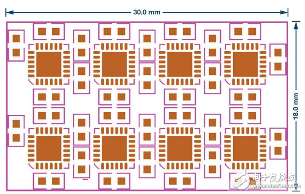
Figure 2. Daisy Chain Switch 4 x 8 Matrix Layout
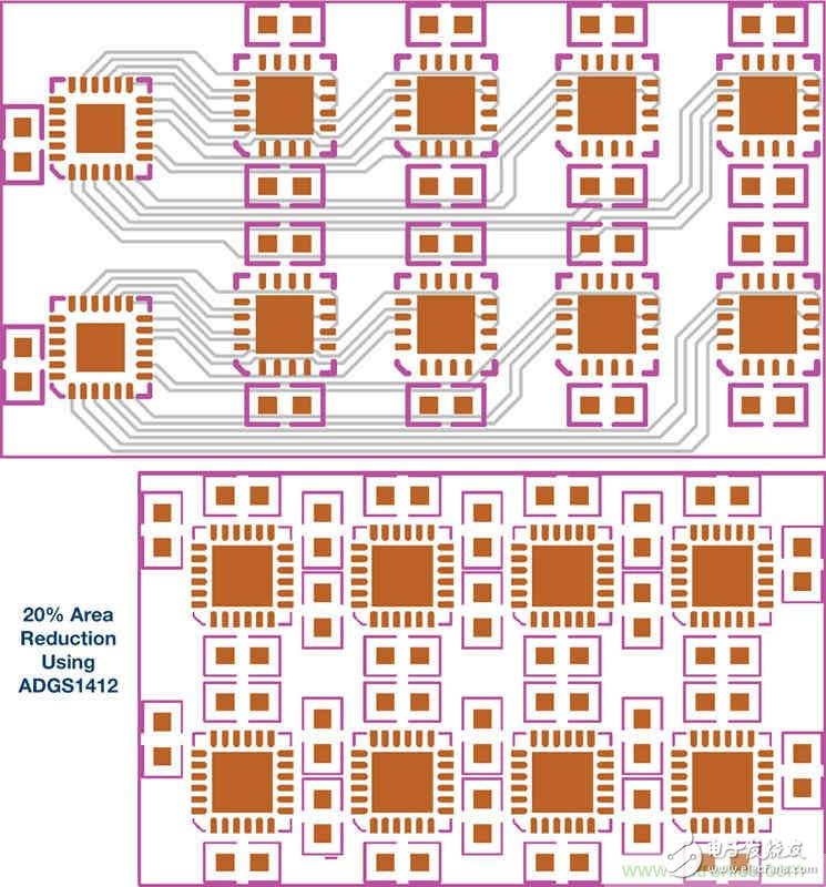
Figure 3. Area comparison of SPI switch and parallel switch solution
ADI SPI Switching CharacteristicsADI's new line of SPI switches can be used to achieve higher channel densities, as shown in the example above. With an innovative stacked two-chip solution (Figure 4), Analog Devices' current industry-leading precision switches can be configured using the industry standard SPI Mode 0 interface. This means not only saves space, but also does not adversely affect system performance. Below is a summary of the main features of the new ADI SPI switch.
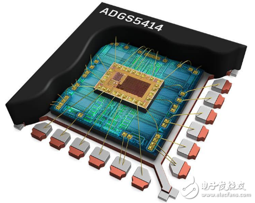
Figure 4. Analog Devices' innovative stacked dual-chip solution
Daisy chain modeAs mentioned above, the ADI SPI switch can operate in daisy-chain mode. The ADGS1412 device connection in a daisy-chain configuration is shown in Figure 5. All devices share the CS and SCLK digital lines, and the SDO of the device is connected to the SDI of the next device. All devices in the daisy chain are daisy-chained with a single 16-bit SPI frame instruction. In daisy-chain mode, SDO is an 8-cycle delayed version of SDI, so the desired switch configuration can be passed from one device in the daisy chain to another.
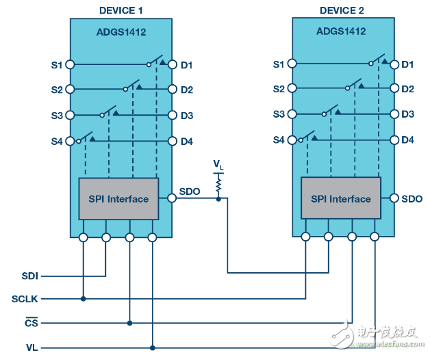
Figure 5. Two switches in a daisy-chain configuration
Error detection functionProtocol and communication errors on the SPI interface can be detected when the device is in Addressing Mode or Burst Mode. There are three error detection methods, SCLK error count, invalid read and write addresses, and up to 3 bits of CRC error detection. These error detection features ensure that the digital interface works reliably even in harsh environments.
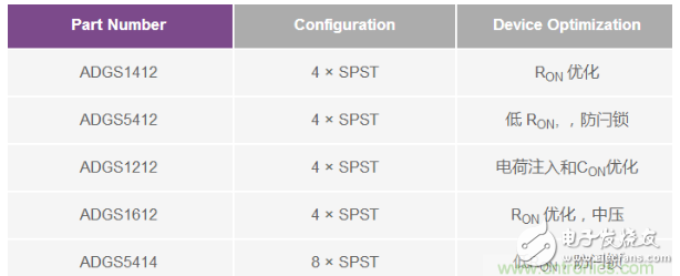
ADI SPI Switch SeriesThe ADGS1412 is the first in a series of SPI switches being developed by Analog Devices. Thanks to the innovative two-chip solution developed by Analog Devices, the ADGS1412 not only has the same best-in-class low RON performance as the parallel control device ADG1412, but also has the advantages of a serial interface.
The series will be built on ADI's high-performance switches, offering an SPI-controlled version of the existing, industry-leading switch. Table 1 lists the current and planned releases of the new ADI SPI switch family. The product model represents which analog switch chip and SPI to parallel converter are multi-chip packaged, and the additional S indicates that it is an SPI control version. These products will be released in 2017.
Table 1. New SDI SPI device optimization products planned
In high channel density applications, there are many advantages to using SPI control switches compared to using parallel control switches. It reduces the board space occupied by each switch, resulting in higher switching density. This is because it reduces the number of digital control lines required and no other devices are needed to provide these control lines.
ADI's innovative precision SPI switching solutions support increased channel density. The daisy-chain mode offered by these devices facilitates these goals. Thanks to the two-chip solution, ADI's industry-leading switching performance of current switching products is passed on to new products. The ADGS1412 is the first in a new line of SPI-controlled switches, and the complete product line will be released in 2017 and 2018.
Organic Light-Emitting Diode Display
Organic Light-Emitting Diode Display,Ultra-Clear Pm Oled Display,Oled Sytip Light,The Oled Display
ESEN Optoelectronics Technology Co., Ltd, , https://www.esenlcd.com