In order to build a new park in Sejong, Chungcheongnam-do, South Korea, the Samsung Group announced its next-generation new business investment plan on January 11, 2010, and plans to invest in energy-saving (including next-generation batteries and LEDs) from 2010 to 2015. In the areas of lighting, health care, etc., the cumulative investment will reach 2.05 trillion won (about 1.8 billion US dollars), and will be Samsung Electronics, Samsung SDI (Samsung SDI), Samsung Electro-Mechanics, Samsung LED (Samsung LED) and five group companies including SDS (Samsung Data System) entered the new park in Sejong City.
The Samsung Group returned to Samsung by the president. On May 11, 2010, the Samsung Group re-launched the green energy and biotechnology new business investment plan. It plans to invest in LED, solar cell, vehicle battery and bio-pharmaceutical in 2010~2020. In the field of medical equipment, the cumulative investment will reach 23.3 trillion won, which will significantly increase investment compared with the plan published in January 2010.
Observing the cumulative total investment of the Samsung Group's Green Energy and Biotech New Business Investment Project from 2010 to 2020 and the 2020 revenue target, LEDs account for a higher proportion than the other four fields, which means that Samsung LED, which dominates the LED business in the Samsung Group, will Continue to actively expand production capacity to accelerate the growth of its revenue.
In 2009, Samsung LED revenues have more than doubled from 2008, reaching 635 billion won, and are expected to grow to 1.6 trillion won in 2010. In terms of capacity expansion, Samsung LED has two factories that will continue to develop its stable LED TV application, and then add the organic metal chemical vapor deposition (MOCVD) required for mass production of LED dies. The equipment, as for its third plant to be built in Sejong, South Korea, will focus on applications other than LED TVs such as LED lighting.

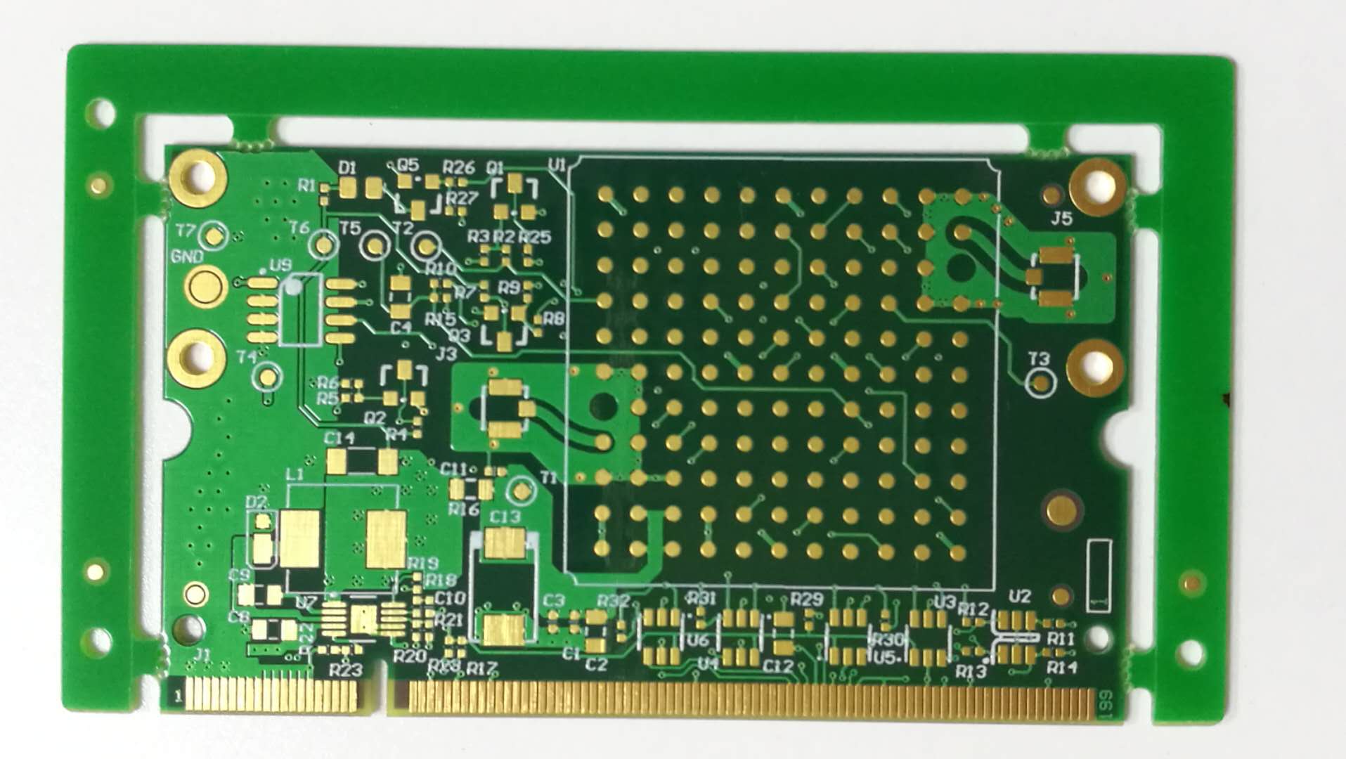
Flash Gold+Hard Gold board. the base Material is FR4 IT180A (TG180). 8-layer PCB.Copper thickness is 1oz inner-layer/1.5oz outer-layer.Board Thickness is 1.8mm and the Min.Hole Size is 0.3mm. Min.Line Width/Min.Line Spacing is 0.25mm/0.25mm. green solder-resist & white silkscreen. E-test: 100%. Flash Gold(hard Gold) is an expensive surface treatment, which has the advantage of being able to withstand friction.

Flash Gold(hard Gold)
Flash Gold,Custom Flash Gold,Hard Gold,Stick Flash Gold
Orilind Limited Company , http://www.orilind.com