Careful selection of devices and good thermal design can help engineers optimize the design of ultra-small DC-DC converters used in mobile devices to achieve increased power density while also ensuring reliability.
Miniaturization of power supply devices
End users need ultra-small devices that can provide rich functions, such as mobile phones, portable media players (PMP) or global positioning system (GPS) devices, etc. Use smaller components. In terms of digital integrated circuits (ICs), implementing Moore's Law allows component manufacturers to significantly reduce chip size while also improving device performance and integration. The replacement products of analog ICs also provide equivalent or higher performance than their predecessors, while the printed circuit board (PCB) has a smaller footprint. Power semiconductor manufacturers are also pursuing miniaturization, using a smaller footprint to provide higher power handling capabilities, thereby providing the highest possible power density.
However, pursuing this goal poses more stringent thermal management challenges for system designers. The energy lost during power conversion is released in the form of heat, and reducing the size of the components (related to the heat generated) will cause the operating temperature to increase. The reason is simple. The smaller the die, the lower the ability to generate heat. The possible adverse effects of miniaturization include low reliability, unpredictable device performance, and device damage in extreme cases. In general, the higher the junction temperature, the higher the probability of device failure.
To successfully use ultra-small power devices in modern portable equipment, it is necessary to pay close attention to the two stages of components and circuit boards to minimize the amount of heat generated in the device and ensure that the heat can be efficiently removed.
Packaging innovation
In order to minimize the heat generated, device designers must first consider high power conversion efficiency. For example, for general-purpose applications such as point-of-load (PoL) regulators, switching converters have advantages over linear converters. The best switching converters can provide peak efficiency in the 95% to 97% range.
In order to be able to dissipate heat effectively, a number of new power supply packages with small form factor have emerged in recent years. These packages are optimized to minimize the thermal impedance between the die and the case, allowing heat to be efficiently removed from the device.
In the latest package for portable applications, such as? DFN or? Subminiature lead-free packages like CSP have exposed metal pads on the bottom. The pad is soldered down to conduct heat directly to the PCB. The package size can be 2mmx2mm or smaller, and devices of this type can provide a continuous current of up to about 1.5 A.
In order to ensure the stable output with the largest possible output current and extend the service life to the longest, when designing with these devices, engineers need to apply reasonable thermal design guidelines and consider the recommendations of device manufacturers in circuit board wiring, etc. .
Calculate power dissipation
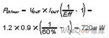
The power dissipation of the switching converter can be calculated using Equation 1:
![]()
Assuming that the voltage regulator produces a fixed output voltage value, the power dissipation is maximum when the output current is maximum and the efficiency is the lowest; and when the ambient temperature is high and the input voltage is the lowest, the energy efficiency will be the lowest.
Analyzing the design of the DC-DC converter can demonstrate how to calculate the necessary power dissipation in the worst case and understand how the power dissipation is related to the package thermal impedance and the maximum allowable ambient operating temperature.
Taking ON Semiconductor's NCP1529 DC-DC converter as an example, the device uses a thermally enhanced 2mmx2mmx0.5mm? DFN-6 package or 3mmx1.5mmx1mm TSOP5 package, suitable for battery-powered equipment. The input voltage range of NCP1529 is 2.7V to 5.5V. It supports single lithium ion battery or 3 alkaline / nickel cadmium / nickel metal hydride batteries. The output voltage can be adjusted from 0.9V to 3.9V, and the maximum output current is 1.0A. In addition, the IC has an internal thermal shutdown circuit to prevent catastrophic damage to the device when the junction temperature exceeds the maximum value. If the temperature reaches 180 ° C, the device will be turned off, and all power transistors and control circuits will also be turned off. When the temperature is below 140 ° C, the device will restart in soft-start mode.
Of course, the best application design should pay attention to reducing the potential probability of a shutdown condition. One of the first tasks to be done is to clearly understand the work efficiency.
We can consider a device that provides a 1.2V IC core voltage with a maximum current of 900mA. Figure 1 shows the operating efficiency of the NCP1529 under different output currents at an ambient temperature of 85 ° C, an input voltage of 2.7V, and an output voltage of 1.2V. When the output current is 0.9A, the working efficiency of the device is 60%.
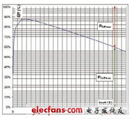
Figure 1 NCP1529 energy efficiency at Vin = 2.7 V, Vout = 1.2 V, and temperature of 85 ℃
Substituting these values ​​into Equation 1 yields the following worst-case expression of power dissipation:
This number is very important and can help us optimize the thermal performance of various applications.
Correlation between power and temperature
Thermal impedance (RθJA) is used to describe the ability of the package to transfer heat from the silicon junction to the outside environment. The lower the thermal impedance, the better the device can transfer large amounts of heat. The expression unit of RθJA is ℃ / W, so we provide a tool for engineers to correlate the electrical power (dissipation) calculated in watts (W) with the temperature in degrees Celsius (℃).
In the data sheets of the latest power devices, it is often claimed that the RθJA value of the device is extremely low. However, if the system designer expects to achieve the expected performance in the end product, he must pay close attention to the circuit board layout and the thermal design of the PCB. The NCP1529 data sheet shows the device's individual RθJA (? DFN-6 package, 220 ° C / W) and the RθJA (40 ° C / W) when this device is used for recommended circuit board layout. These figures show that PCB design has a significant impact on thermal impedance. In fact, following the device manufacturer ’s recommendations can reduce the effective RθJA by a factor of five.
Knowing RθJA and PDIP (max), you can use the following equation to calculate the maximum ambient temperature the application can withstand:
![]()
Here, TJmax is the maximum junction temperature that the device can withstand (the temperature corresponding to NCP1529 is 150 ° C).
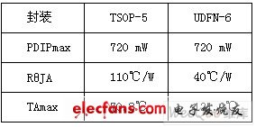
It should be noted that NCP1529 provides both TSOP-5 and? With the DFN-6 package, we can quickly determine the impact of each package selection on performance. Table 1 summarizes the power dissipation of various packages, package thermal impedance and calculated maximum ambient temperature.
Table 1 shows that for converters to work satisfactorily at the highest ambient temperature, package selection is an important issue.
Table 1: Data conversion between electrical and thermal domains
Another way to estimate the impact of package thermal characteristics on application performance is to examine the power drop curve. Figure 2 shows the NCP1529 curve, detailed? The relationship between the maximum ambient temperature threshold of DFN-6 and TSOP-5 packages and power dissipation.
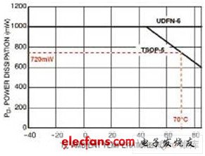
Figure 2 IC power drop characteristic curve
When the ambient temperature is lower than 70 ℃, TSOP-5 and? The DFN-6 package can dissipate 720mW of power, so it can meet the worst-case requirements for this application. however,? The power dissipation capability of the DFN-6 package is stronger, and it can withstand higher temperatures than the equivalent converter design in the TSOP-5 package.
? The performance advantage of the DFN-6 package is due to its thermally enhanced structure, and the exposed metal pad significantly reduces the thermal impedance from the die to the PCB.
About Silicone Camera Case
As we konw,the people more and more like take picture and the camera is hot selling in the market.In the same time,the Camera Protector Case are invented.In the camera case market,it has soft case and the hard case.Our factory is wholesales silicone Soft Camera Case .Silicone camera case has many advantages,it is not only can prevent nails from being scratched and worn for a long time, and can protect the screen and the buttons,but also has anti-skid effect,the silicone case texture is soft and comfortable,this will make you take a better picture!
Silicone Camera Case introduction:
1.Product name:Soft camera case,silicone camera case,camera protector case,Small Camera Case,Silicone Camera Cover, Camera Sleeve
2.Place of origin:Guangdong China
3.Color:any pantone color
4.Logo:Printing,debossed,embossed
5.MOQ:500pcs.
6.Package:1 pcs/opp,customized design is available.
7.Design:Customized/stock
8.Certification:FDA,LFGB,SGS,ROHS,etc.
9.Usage:Protect camera/Decoration.
10.Silicone Camera Case photo's for reference.

Silicone Camera Case
Soft Camera Case,Silicone Camera Case,Camera Protector Case,Small Camera Case,Silicone Camera Cover,Camera Sleeve
OK Silicone Gift Co., Ltd. , https://www.oemsiliconegift.com