1 Introduction With the advancement of technology, TFT LCD as a display device has been more and more widely used in various embedded systems. TFT LCD module with touch screen can not only provide high-quality screen display for human-machine interface in system application, but also provide more intuitive and convenient interactive input. TMT035DNAFWU1 is an 8.89 cm (3.5 in) TFT LCD module produced by Shenzhen Tianma Microelectronics Co., Ltd. This module has a built-in LCD driver and integrates a four-wire resistive touch screen and backlight circuit. S3C2440A is a 32-bit embedded RISC (reduced instrucTIons set computer) microprocessor based on the ARM920T core designed by Samsung. It has a maximum operating frequency of 533 MHz and integrates a general-purpose LCD controller, 8-channel 10-bit ADC and touch screen interface, and has the advantages of high performance and low power consumption, suitable for smart phones, portable media players, handheld navigators and other fields. This article is based on the S3C2440A embedded system, using TMT035DNAFWU1 as the display device, designed the TFT LCD drive circuit, and completed the debugging of the drive display effect under Linux.
2 TFT LCD interface timing The display resolution of TMT035DNAFWU1 is 320 × 240, using 24-bit digital RGB interface, which can display 16.7 M colors.
The RGB interface is designed to provide high-quality display for TFT LCD modules. The interface can complete animation display at high speed and low power consumption. It includes 4 important control signals VSYNC, HSYNC, DCLK and VDEN, which are used for frames , Line, pixel data transmission.
Figure 1 is a timing diagram of the RGB interface of the TMT035DNAFWU1 module.
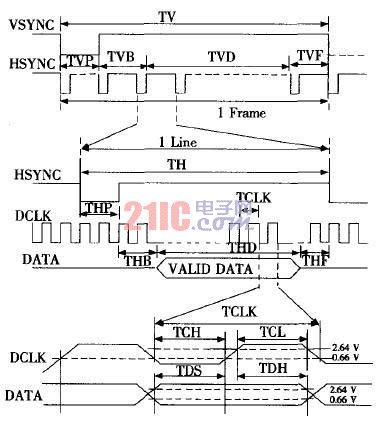
Figure 1 RGB interface timing diagram
3 S3C2440A LCD Controller Introduction The S3C2440A built-in LCD controller can transfer the data displayed on the LCD from the internal data buffer of the system to the external LCD driver through the logic unit. It can support displays with different resolutions, such as 640 × 480, 320 × 240, etc., and can support a maximum of 16.7 M color TFT module with 24-bit data. Its controller block diagram is shown in Figure 2.
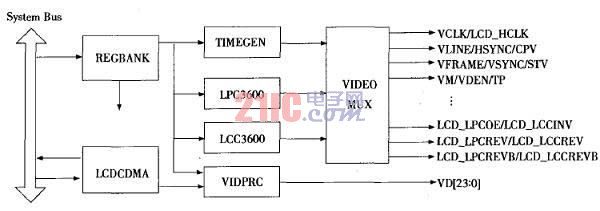
Figure 2 S3C2440A LCD controller block diagram
3.1 General control block diagram The LCD controller is mainly composed of REGBANK and LCDCDMA, which are used to generate the necessary control signals and transmission data signals, as shown in Figure 2. REGBANK has 17 programmable register sets and 256 × 16 palette memory, used to set the LCD controller. LCDCDMA is a dedicated DMA (Direct Memory Access) that automatically transfers video data from the frame memory to the LCD controller. The video data can be directly displayed on the screen without being processed by the CPU. TIMEGEN is composed of programmable logic devices and generates VFRAME / VSYNC, VLINE / HSYNC, VCLK / DCLK, VM / VDEN signals, etc., to support different LCD driver interface timing and speed. LPC3600 and LCC3600 are dedicated LCD controllers and will not be described in detail here.
3.2 Introduction of TFT controller By configuring LCDCON1 / 2/3/4/5 in REGBANK register set, TIMEGEN generates programmable control signals to support different types of LCD drivers.
The VSYNC and HSYNC pulses are related to the settings of LCDCON2 / 3's HOZVAL and LINEVAL. The values ​​of HOZVAL and LINEVAL are determined by the resolution of the LCD screen, as follows:
HOZVAL = (Horizontal display size) -1 (1)
LINEVAL = (VerTIcal display size) -1 (2)
The frequency of VCLK depends on the setting of CLKVAL in LCDCON1, configured in LCDCON1, the relationship between VCLK and CLKVAL is as follows (the minimum value of CLKVAL is 0):
VCLK (Hz) = HCLK / [(CLKVAL + 1) × 2] (3)
HCLK is the clock signal generated by the PLL clock generator in S3C2440A.
The frequency of VSYNC is the frame frequency, which is related to LCDCON1 / 2/3/4, the calculation formula is as follows:
Frame Rate = 1 / {[(VSPW + 1) + (VBPD + 1) + (LINEVAL + 1) + (VFPD + 1) 1 × [(HSPW + 1) + (HBPD + 1) + (HFPD + 1) + (HOZVAL + 1)] × [2 × (CLKVAL + 1) / (HCLK)]} (4)
The setting method of each parameter value of formula (1) ~ (4) is given in §5.2.
4 Drive circuit design In addition to the data transmission signal interface, the drive circuit of the TFT LCD module also includes the power circuit, VGL, VGH, and VCOM voltage circuit provided to the module. According to the interface of the TFT LCD module and the output pin of the controller embedded in the S3C2440A, the control circuit design of the LCD display is completed. The circuit interface design is shown in Figure 3.

5 Driver software design under Linux
5.1 Frame Buffer Device Frame buffer is a driver interface in Linux 2.2.XX and above kernel. The interface uses mmap system calls to abstract the display device as a frame buffer, allowing upper-layer applications to directly read, write, and I / O control operations to the display buffer in graphics mode. The frame buffer device belongs to the character device, and adopts the interface mode of "file layer-drive layer".
5.2 LCD driver design The main work of the TFT LCD driver design includes: initializing the LCD controller LCDCON1 ~ 5 of the S3C2440A, setting the display mode and color number by writing registers, and then allocating the LCD display buffer. According to the timing and display requirements of the TMT035DNAFWU1 interface, the screen display resolution is Horizontal display size = 320, Vertical display size = 240, VCLK = 6.4 MHz, and HCLK = 133 MHz, so CLKVAL = 9. The buffer size is: number of dot matrix lines × number of dot arrays × number of bits used to represent one pixel / 8. The buffer is usually allocated in a large-capacity off-chip SDRAM. The start address is stored in the LCD control register. The display buffer to be allocated is 150 kB. Finally, initialize an fb_info structure, fill in the member variables, and call register_framebuffer (struct fb_info * fb info) in fbmem.C to register fb_info into the kernel.
5.3 RGB interface display parameter adjustment The LCD control register of S3C2440A mainly includes: LCDCON1 ~ 5. LCDCON1 can set the type of LCD, the number of data bits, whether VDEN output and DCLK are required; LCDCON2 mainly sets VBPD, VFPD, VSPW; LCDCON3 and LCDCON4 set HBPD, HFPD, HSPW; LCDCON5 can set DCLK, HSYNC, Set the polarity of VSYNC. Figure 4 is a schematic diagram of the working principle of the RGB interface display. The effect of each parameter in the actual display is shown in Figure 4.
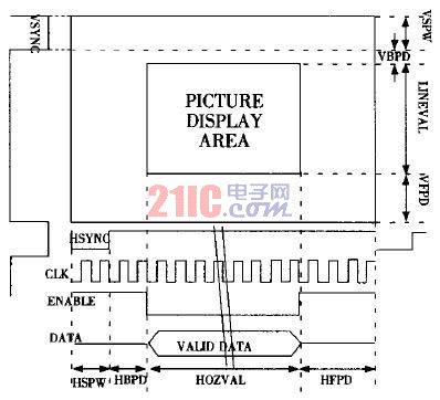
Figure 4 RGB interface display working principle In Figure 4, the final display area (DISPLAY AREA) is composed of pixel clock signal (DCLK), line synchronization signal (HSYNC), frame synchronization signal (VSYNc), data enable signal (VDEN / ENABLE) As a result of the joint action, its size and position are determined by the actual configuration of the parameters. Among them, HSPW, HBPD and HFPD determine the row effective data information of the display area, and VSPW, VBPD and VFPD determine the frame effective data information in the display area.
Based on the driver display program under Linux, the following is part of the source code for successful debugging:
/******s3c2440fb.c******/
#define H_SW 35;
#define H_FP 15;
#define H_BP 30;
#define V_SW 5;
#define V_FP 5;
#define V_BP 10;
...
static struct s3c2440fb_mach_info xxx_stn_info __initdata = {
pixclock: PIXEL_CLOC, hpp: PIXEL_BPP,
xres: H_RESOLUTION, yres: V_RESOLUTION,
hsync_len: H_SW, vsync_len: V_SW,
left_margin: H_BP, upper_margin: V_BP,
right_margin: H_FP, lower_margin: V_FP,
sync: 0, cmap_static: 1,
reg: {
lcdcon1: LCD1_BPP_16T | LCD1_PNR_TFT | LCD1_CLKVAL (12),
lcdcon2: LCD2_VBPD (V_BP) | LCD2_VFPD (V_FP) | LCD2_VSPW (V_SW),
lcdcon3: LCD3_HBPD (H_BP) | LCD3_HFPD (H_FP),
lcdcon4: LCD4_HSPW (H_SW),
lcdcon5: LCD5_FRM565 | LCD5_INVVLINE | LCD5_INVVFRAME | LCD5_HWSWP | LCD5_PWREN,
},
};
In the actual driver writing process, the parameters of different TFTLCD modules will be different, so the relevant parameters need to be adjusted according to the effective position of the actual data. Figure 5 is a comparison diagram of the system display before and after the adjustment of the RGB interface parameter configuration. If the HSPW, HBPD and HFPD are not correctly allocated in the software initialization setting, the position of the row effective data will be misaligned, which is shown in the actual display as the overall left and right offset of the displayed image, as shown in Figure 5 (a) , LCD display screen shifted to the left. Similarly, if the VSPW, VBPD, and VFPD are not configured correctly, the position of the valid data in the frame data will be misaligned, which is manifested in the actual display as the vertical deviation of the displayed image.
5.4 Touch screen driver design Set the touch screen interface to wait for interrupt mode (INT_TC interrupt), if an interrupt occurs, immediately activate the corresponding AD conversion. The conversion mode generally selects the separate X / Y axis coordinate conversion mode or the automatic (continuous) X / Y axis coordinate conversion mode to obtain the X / Y coordinates of the touched point. After obtaining the X / Y axis coordinate value of the touched point, it returns to the wait interrupt mode. The driving process of the touch screen is shown in Figure 6.

Figure 6 Flow chart of touch screen control The touch screen device is also defined as a character device in the Linux system. You need to set the global variable struct TS_DEV in the touch screen device driver. This variable is used to save the related parameters of the touch screen: the message queue waiting to be processed , The current sampling data, the last sampling data and other information, the variables are defined as follows:
typedef struct {
unsigned int penStatus;
/ * PEN_UP, PEN_DOWN, PEN_SAMPLE * /
TS_RET buf [MAX_TS_BUF];
/ * Ring buffer * /
unsigned int head, tail;
/ * Head and tail of ring buffer * /
wait_queue_head_t wq;
spinlock_t lock;
} TS_DEV;
According to the resolution of the TFT LCD corresponding to the touch screen, the size of the ring buffer is initialized and configured.
6 Conclusion The working sequence of the TFT LCD module interface of the RGB interface is analyzed. Taking the S3C2440A processor of the ARM920T core as the core, the corresponding driver circuit is built with the peripheral circuit, the Linux display driver development is completed, and the system displays a clear and stable display. The design of the driving circuit of the TFT LCD module with touch screen and the adjustment method of the display effect provide a complete set of solutions for the design of embedded systems such as various handheld digital electronic products and navigators.
Hand Mixers are machines that can whisk eggs and cream to solid or mix dough. Hand mixers including just hand mixers and hand mixers with bowl. In addition, hand mixers with bowl can divided into hand mixers with rotary plastic bowl and hand mixers with rotary S/S bowl. Usually, hand mixers with bowl are more convient and effiency, they can not only beat eggs and cream, but also can mix dough and do not to hold the hand all the time.

Hand Mixers
Hand Mixers,Stand Mixer,Kitchen Hand Mixer,Electric Mixer
Flying Electronic Co., Ltd , https://www.flyingelectronic.com